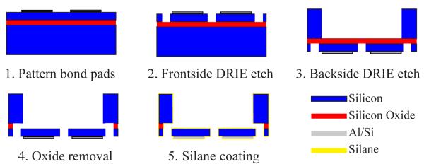
Figure 3.

Fabrication steps for the ASC begin with an SOI wafer having a highly-doped 15 μm device layer and an undoped 400 μm handle wafer. Here the schematic is shown for a single device on the SOI wafer. (1) After patterning 99% Al-1% Si bond pads, (2) DRIE defines the comb structure on the frontside and (3) open regions on the backside directly under the floating structures. (4) The 1 μm buried oxide layer is wet etched away and the entire SOI wafer is dried via critical point drying. (5) Individual devices are removed from the SOI wafer and are coated with a protective layer of HMDS silane.
