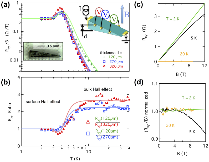
Figure 1. Surface Hall effect.
(a), Markers, Hall resistances Rxy divided by magnetic field B versus temperature T at three different thicknesses d in a wedge shaped sample S1. Lines are simulations using a two conduction channel model (see text). Left inset, picture of the crystal before wiring. Right inset, measurement schematic. (b), Markers, ratios between Hall resistances Rxy at different d, showing the transition from bulk to surface conduction as temperature is lowered. Lines are calculated from simulations as in (a). (c), Rxy versus B at various T for d = 120 μm, showing nonlinearity at around 5 K. (d), Rxy/B normalized to small field values to demonstrate the nonlinearity.

