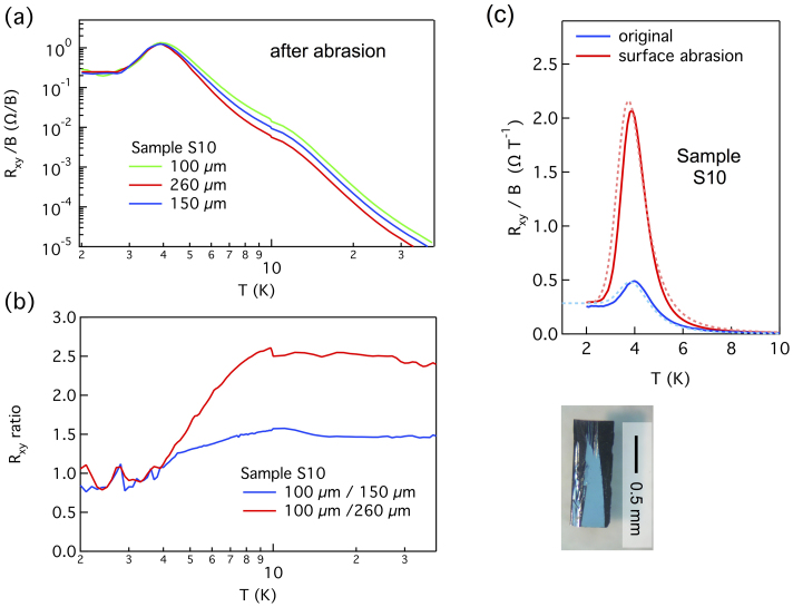
Figure 3. Surface conduction after surface treatments.
(a), Markers, Hall resistances Rxy divided by magnetic field B versus temperature T at three different thicknesses d in a wedge shaped sample S10, after intentional chemical etching and cutting. (b), Markers, ratios between Hall resistances Rxy at different d, showing the transition from bulk to surface conduction as temperature is lowered. (c), Solid lines, Hall resistance Rxy divided by magnetic field B versus temperature T, before and after surface abrasion. Dashed lines are simulations assuming abrasion only reduces the effective surface mobility μS. Inset, picture of sample S10 during abrasion.

