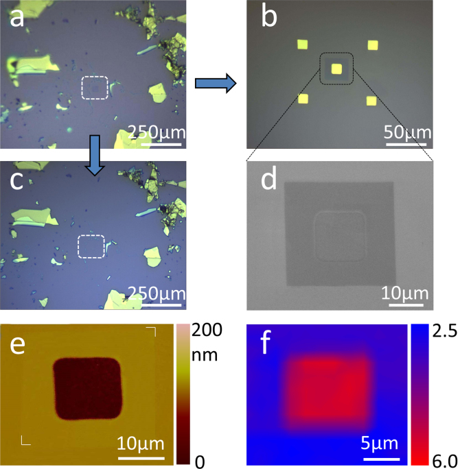
Figure 2. Results of the selective transfer and precise location.
(a-c), Optical images of (a) a monolayer MG patterned by femtosecond laser on a SiO2/Si wafer, (b) the patterned graphene located on a chosen microcavity obtained by selective transfer, and (c) the graphene/graphite flakes remaining on the original substrate. (d-f), The morphological images of the patterned graphene above the microcavity analyzed by (d) SEM, (e) AFM, and (f) Raman mapping with a 2D- to G-band intensity ratio.

