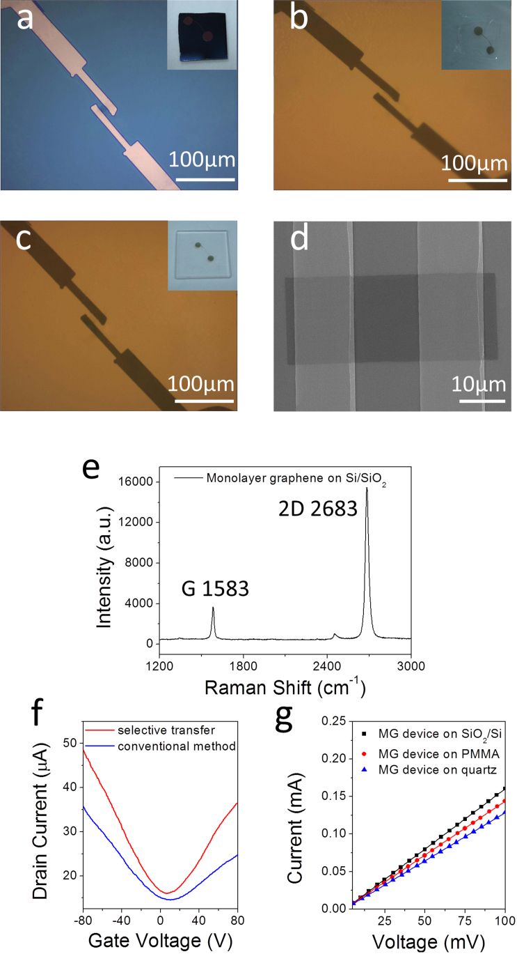
Figure 4. The fabrication and transfer of the graphene FET with graphene/electrodes structure.
(a-c), Optical images of the graphene device on (a) Si/SiO2, (b) PMMA, and (c) quartz. (d), SEM image of the patterned graphene transferred onto the Au electrodes to fabricate the device. (e), The Raman spectrum of the transferred graphene on a Si/SiO2 wafer. (f), The transfer characteristic curves of the two graphene FETs fabricated via the selective transfer and conventional methods. (g), The current as a function of the voltage for the graphene device fabricated by the selective transfer during the device transfer process.

