Fig. 2.
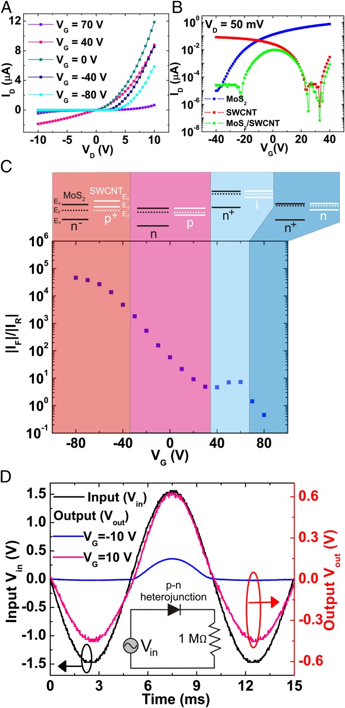
Electrical properties of the s-SWCNT/SL-MoS2 p-n heterojunction diode. (A) Gate-tunable output characteristics showing the transition from a nearly insulating state at VG = 70 V to a conductive state with relatively poor rectification at VG = 40 V to a highly rectifying diode behavior at negative gate voltages. (B) Transfer characteristics of the p-n junction (green), showing an antiambipolar characteristic, which is qualitatively a superposition of the transfer characteristics of the p-type s-SWCNT FET and n-type SL-MoS2 FET. (C) Forward-to-reverse current ratio (at a heterojunction bias magnitude of 10 V) as a function of gate bias. The labels at the top show the corresponding band diagrams for the s-SWCNT/SL-MoS2 p-n heterojunction. At a high positive gate bias, the formation of an n+-n junction implies a low rectification ratio that transitions into an n+-i junction (plateau region in the plot) with reducing VG. The rectification ratio then rises with decreasing gate bias due to the formation of a p-n junction. (D) Demonstration of gate-tunable rectification using the p-n heterojunction diode. The y axis on the left shows the input voltage, whereas the y axis on the right shows the output voltage across the series resistor (1 MΩ). As a function of the gate bias, the device evolves from a nonrectifying resistor-like state at VG = 10 V (magenta) to a diode-like rectifying state at VG = -10 V (blue).

