Fig. 3.
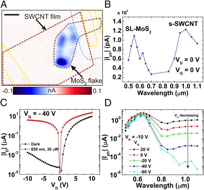
Photoresponse of the p-n heterojunction. (A) Scanning photocurrent micrograph of a representative heterojunction device acquired at VD (s-SWCNT electrode), VG = 0 V showing the outlines of the SL-MoS2 flake (purple dashed line) and the patterned s-SWCNT film (red dashed line) acquired at 700 nm with 20-μW power. Regions of large negative photocurrent (blue) are observed in the overlapping junction region. The patterned alumina and electrodes are indicated by cyan and yellow dashed lines, respectively. (B) Photocurrent spectrum of the junction under global illumination and zero bias conditions. The photocurrent magnitude is highest at the characteristic absorption energies of both SL-MoS2 and s-SWCNTs. The photocurrent spectrum is acquired at the same incident power (30 μW). (C) Output curve of the same device in the dark and under global illumination at 650 nm. (D) Photocurrent spectral response can be tuned with the gate voltage. With decreasing gate voltage, the increased p-doping of the nanotubes and concomitant decreased n-doping of MoS2 leads to a lower photocurrent in the near infrared region.

