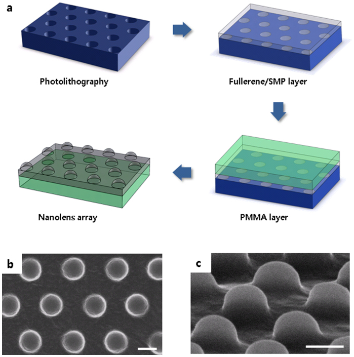
Figure 1. Fullerene embedded nanolens array.
(a), Schematic diagram of preparation procedure for the nanolens array. Nanostructure is generated on the silicon template using photolithography. The SMP solution, where fullerenes are suspended, is cast on the nanopatterned template. In addition, a PMMA layer is fabricated, followed by detaching the nanolens array from the silicon template. (b), (c), SEM images of the nanolens array ((b) top view and (c) tilt view). The scale bars indicate 200 nm.

