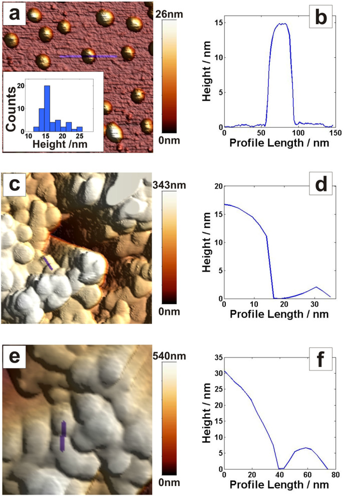
Figure 2. Atomic force microscopy studies of AuNPs and 3D nanostructured electrodes.
Images and corresponding height profiles of (a, b) AuNPs on a poly-lysine-coated mica surface, (c, d) microelectrode coated with AuNPs, (e, f) the microelectrode from panels c and d, after electrochemical cleaning. Scan areas for all images were 400 nm × 400 nm. Note that the height measured with AFM represents the diameter of the NPs; the width does not represent the diameter due to tip dilation effects57.

