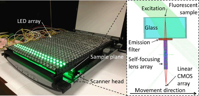
Fig. 1.
(Left) Experimental setup for the high-throughput fluorescent imaging platform combining a flatbed scanner, a custom-designed absorption filter, and a two-dimensional array of external light sources for computer-controlled and high-angle fluorescent excitation. The setup is capable of taking fluorescent measurements over a FOV of ~532 cm2 in less than 5 minutes. (Right) Schematic diagram of the light path inside the scanner head. The excitation light (green) arrives at a ~45° angle, and excites the fluorescent sample. The excitation does not reach the linear CMOS sensor of the scanner due to the low NA of the self-focusing lens array. The light scattered by the sample is attenuated by the emission filter, while the fluorescent emission passes through it. The gradient index lens array focuses the fluorescent light emitted by the sample onto the CMOS array.

