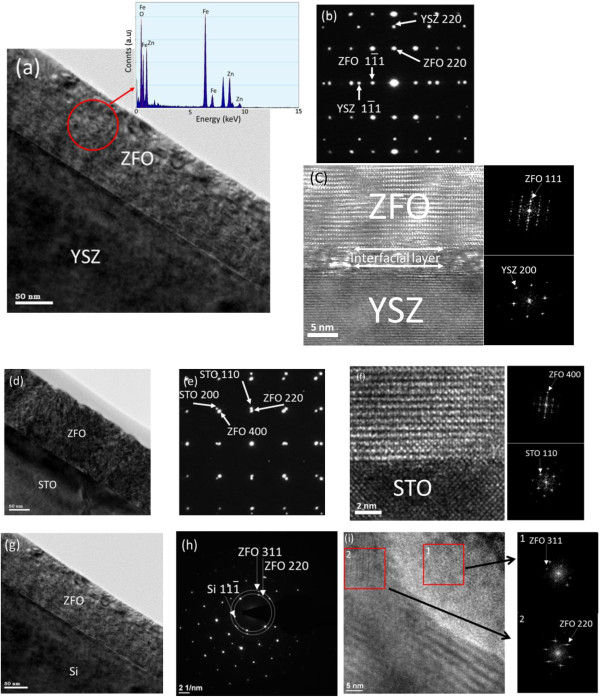
Figure 4.

TEM analysis results of the ZFO film on the YSZ, STO, and Si. (a) Low-magnification TEM image of the ZFO film on the YSZ. The EDS spectra taken from the film were also displayed. (b) The selected area electron diffraction pattern from the ZFO film and YSZ. (c) HRTEM images and corresponding FFT patterns taken from the various regions of the sample. (d) Low-magnification TEM image of the ZFO film on the STO. (e) The selected area electron diffraction pattern from the ZFO film and STO was also presented. (f) HRTEM image taken from the ZFO film-STO interfacial region. (g) Low-magnification TEM image of the ZFO film on the Si. (h) The selected area electron diffraction pattern from the ZFO film and Si. (i) HRTEM images and corresponding FFT patterns taken from the ZFO film grown on the Si.
