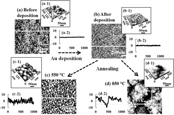
Figure 1.

Illustration of self-assembled Au droplet fabrication process on Si (111). (a) shows AFM images of bare Si (111) and (b) shows the morphologies after 2-nm Au deposition before annealing. (c) and (d) present the surface morphologies of samples annealed at 550°C and 850°C, respectively. AFM top views in (a) to (d) are 1 × 1 μm2 and AFM side views of insets (a-1) to (d-1) are 250 × 250 nm2.
