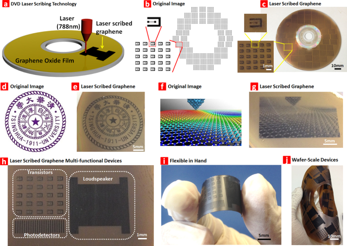
Figure 1. Scalable fabrication of laser scribed graphene.
(a) A schematic diagram showing the fabrication process of laser scribed graphene. A GO film is coated on a DVD media disc. The disc is inserted into a LightScribe DVD drive and a computer-designed circuit is etched onto the film. The laser inside the drive converts the golden-brown GO into black graphene at precise locations. The laser scribing technology makes it possible that the large-area of precise graphene patterns can be obtained in ~25 minutes. (b) An original image of wafer-scale in-plane transistor patterns and (c) the same image reproduced by laser scribed graphene. (d) An original image of Tsinghua University logo [copyright permission from Tsinghua University] and (e) the same image reproduced by laser scribed graphene. (f) A standard complex colored image of graphene and (g) the same image reproduced by reducing graphite oxide at various levels, which corresponds to a change in electrical properties. (h) An array of graphene transistors, an array of photodetectors, and a graphene loudspeaker device integrated in a flexible substrate by the direct laser scribing method. (i) The devices on PET substrate with flexible. (j) Wafer-scale fabrication flexible graphene-based devices.

