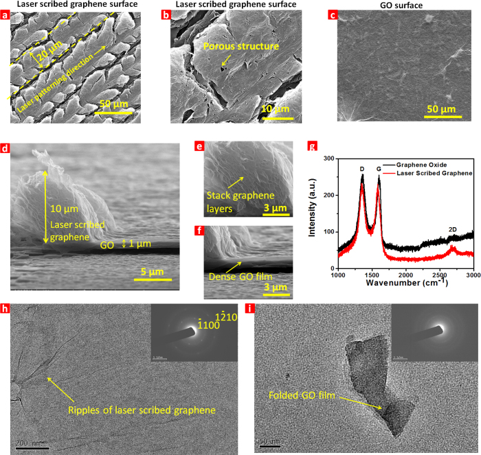
Figure 2. The morphology and structure of the laser scribed graphene and GO film.
(a) The SEM image of laser scribed graphene surface under low magnification. The laser scanning direction is shown. And the minimum patterning resolution of laser scribed graphene is 20 μm. (b) The SEM image of laser scribed graphene surface under high magnification. (c) The surface profile of GO film under SEM. (d) Cross-sectional view of GO and laser scribed graphene film. An increase in laser scribed graphene film thickness is clearly visible. (e) The zoom-in cross-sectional view of laser scribed graphene film under high magnification. An stack graphene layers could be clearly indentified. (f) The zoom-in cross-sectional view of GO film under high magnification. (g) The Raman spectrum of the GO (black line) and laser scribed graphene (red line). Compared with GO, the increase in 2D band of laser scribed graphene indicates that few-layers graphene generated after laser irradiation. (h) A TEM image of single-layer laser scribed graphene deposited on carbon TEM grids. Electron diffraction on the graphene film is shown as an inset. (i) A TEM image of few-layer GO film deposited on carbon TEM grids. Electron diffraction on the GO film is shown as an inset.

