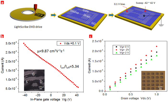
Figure 4. Schematic diagrams and experimental results for a laser scribed graphene in-plane transistors.
(a)Schematic diagram of the fabrication process and testing condition for a laser scribed in-plane graphene transistor. (b) Transfer characteristic for the in-plane graphene transistor with 0.1 V applied bias voltage Vds. Inset showing the in-plane transistor with three-terminal probing. (c) Ids–Vds cure recorded for different values of in-plane gate voltage Vig. The inset is a 5 × 5 array of the in-plane graphene transistor.

