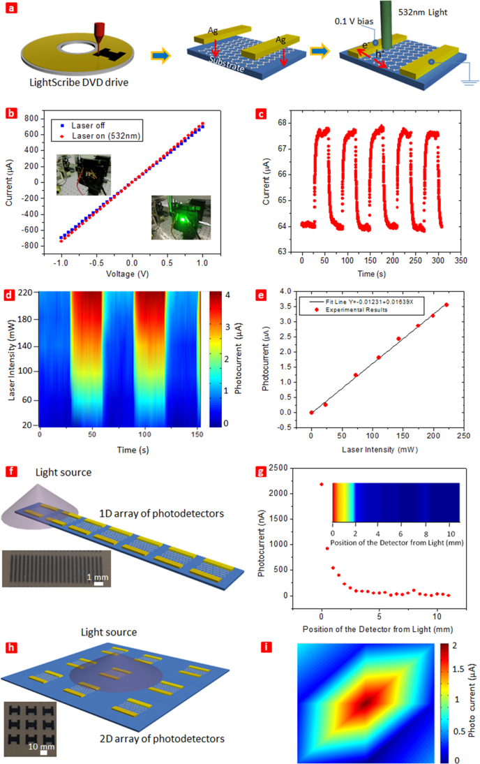
Figure 5. Schematic diagrams and experimental results for laser scribed graphene photodetectors.
(a) Schematic diagram of the fabrication process for a laser scribed graphene photodetector. (b) The I-V cures under laser on and off. Compared with dark line, it indicates that the positive photocurrent generated when apply light. The inset showing the experimental setup for testing the photo detector. The length and the width of the photodetector is 5 mm and 10 mm, respectively. (c) The time versus current under dark and light cycling. Both the dark and light last 30 s for each cycle. When applying light, it is noticed that the photocurrent increase and become saturate in a short time. After dark, the photocurrent decrease and back to original state. (d) The photocurrent mapping by changing photo intensity. Both the dark and light last 30 s for each cycle. It is indicated that larger photo intensity could induce higher photo current. (e) The plot of the photo intensity versus the photo current. The line shows that the photo current increases linearly with the increasing of the photo intensity. (f) Schematic structure of a line array of the photodetectors under a light source put at one end of the array. Inset showing the real photo the 23 pixels array. The length and width of the device are 250 μm and 3000 μm, respectively. The center to center spacing with each devices is 500 μm. (g) Photo current versus the position of the detector from the light. The inset showing the 1-dimensional pixilation plot, where each pixel is represented by a device in the array. The photocurrent is decreased with the increasing the distance from the light source. (h) Schematic structure of a 2-dimentional array of the photodetectors under a light source put at center of the array. Inset showing the real photo the 3 × 3 pixels array. (i) 2-dimensional pixilation plot of the 3 × 3 array.

