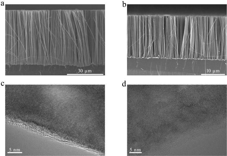
Figure 2. SEM and TEM images of SiNWs prepared by graphite substrate-enhanced MCEE of silicon in aerated aqueous HF solution.
(a), Cross-sectional SEM image of SiNW array prepared on 1–10 Ω · cm p-Si(100) wafer. (b), Cross-sectional SEM image of SiNW array prepared on 2–3 Ω · cm n-Si(100) wafer. (c), High-resolution TEM image of a Si nanowire from 1–10 Ω · cm p-Si(100) wafer. (d), High-resolution TEM image of a Si nanowire from 2–3 Ω · cm n-Si(100) wafer.

