Fig. 19.

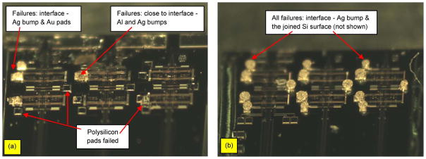
(a) Failed sample failure on the base die showing three kinds of failures. (b) Failed sample on the second die showing one type of failure at the interface between Ag bump and the joined Si bare die surface (not shown).

(a) Failed sample failure on the base die showing three kinds of failures. (b) Failed sample on the second die showing one type of failure at the interface between Ag bump and the joined Si bare die surface (not shown).