Figure 2.

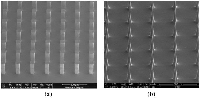
SEM images of (a) the 15 × 15 Si pillar array after DRIE; and (b) Si microneedle array after wet etch process. The scale bar shows 500 μm.

SEM images of (a) the 15 × 15 Si pillar array after DRIE; and (b) Si microneedle array after wet etch process. The scale bar shows 500 μm.