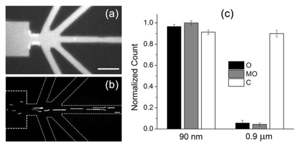
Figure 3.

a) Fluorescence microscopy snapshot showing the 90 nm beads distributed in all outlet channels when −60V is applied to the center outlet (−20V to all other outlets). b) Fluorescence microscopy snapshot of the 0.9 μm beads focusing at the same potential scheme as in (a). Scale bar is 50 μm. c) Quantified particle distributions in each outlet channel for both particle sizes as measured by fluorescence intensity for the 90 nm beads and particle counting of 0.9 μm beads (see experimental section for details). A relatively equal distribution is seen for 90 nm beads whereas 90% of the 0.9 μm beads focus into the center outlet. Error bars represent the standard deviation.
