Figure 3.

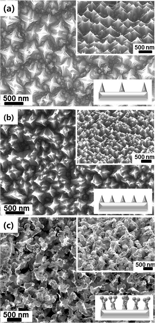
FESEM images and schematics of the Si nanostructures. Etching done at (a) 1,350°C, (b) 1,200°C, and (c) 1,100°C. Insets: tilted FESEM images and schematics of the Si nanostructures.

FESEM images and schematics of the Si nanostructures. Etching done at (a) 1,350°C, (b) 1,200°C, and (c) 1,100°C. Insets: tilted FESEM images and schematics of the Si nanostructures.