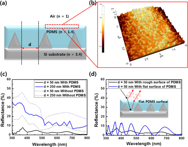
Figure 6.
Schematic of Si nanostructure, AFM image of the PDMS surface, and FDTD-simulated reflectance spectra. (a) The schematic of buffer layer deposition on the non-compact nanopyramids array. (b) AFM image of the PDMS surface after the deposition on the Si nanostructures. The width and height of the Si nanopyramid are 300 and 250 nm in the simulation, respectively. FDTD-simulated reflectance spectra from the air-Si interface (c) before and after the PDMS deposition with increase in the distance between neighboring nanopyramids and (d) with rough and flat surfaces of PDMS. Inset: schematic of the flat PDMS surface on Si nanostructures.

