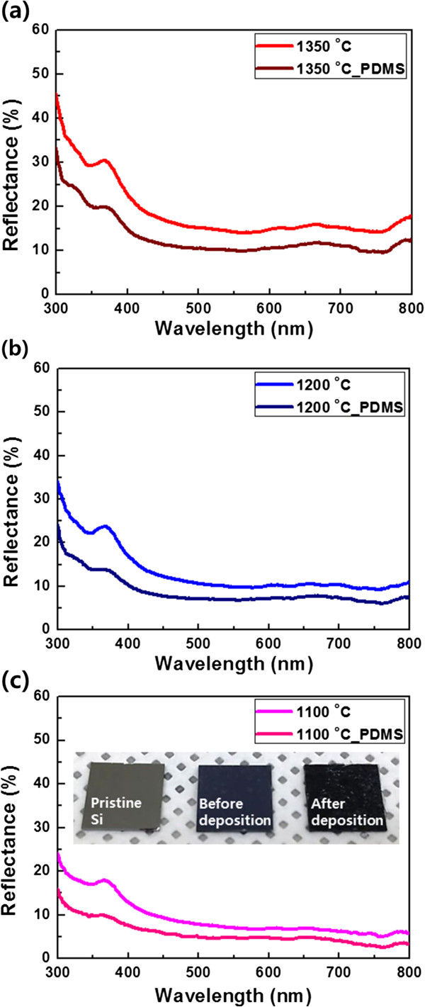
Figure 7.

Reflectance spectra before and after the PDMS deposition on the Si nanostructures. Etching done at (a) 1,350°C, (b) 1,200°C, and (c) 1,100°C. Inset: optical image of the pristine Si and the Si nanostructures (etched at 1,100°C) before and after the PDMS deposition.
