Abstract
Electrical tuning of magnetism is of great fundamental and technical importance for fast, compact and ultra-low power electronic devices. Multiferroics, simultaneously exhibiting ferroelectricity and ferromagnetism, have attracted much interest owing to the capability of controlling magnetism by an electric field through magnetoelectric (ME) coupling. In particular, strong strain-mediated ME interaction observed in layered multiferroic heterostructures makes it practically possible for realizing electrically reconfigurable microwave devices, ultra-low power electronics and magnetoelectric random access memories (MERAMs). In this review, we demonstrate this remarkable E-field manipulation of magnetism in various multiferroic composite systems, aiming at the creation of novel compact, lightweight, energy-efficient and tunable electronic and microwave devices. First of all, tunable microwave devices are demonstrated based on ferrite/ferroelectric and magnetic-metal/ferroelectric composites, showing giant ferromagnetic resonance (FMR) tunability with narrow FMR linewidth. Then, E-field manipulation of magnetoresistance in multiferroic anisotropic magnetoresistance and giant magnetoresistance devices for achieving low-power electronic devices is discussed. Finally, E-field control of exchange-bias and deterministic magnetization switching is demonstrated in exchange-coupled antiferromagnetic/ferromagnetic/ferroelectric multiferroic hetero-structures at room temperature, indicating an important step towards MERAMs. In addition, recent progress in electrically non-volatile tuning of magnetic states is also presented. These tunable multiferroic heterostructures and devices provide great opportunities for next-generation reconfigurable radio frequency/microwave communication systems and radars, spintronics, sensors and memories.
Keywords: multiferroic heterostructures, magnetoelectric coupling, non-volatile
1. Introduction
In the past decade, the ever-increasing demand for faster, smaller and ultra-low power electronic devices propelled the exploration of controlling spin degree of freedom and magnetic states by using electric field (E-field) instead of current [1–7]. For example, state-of-the-art radiofrequency (RF)/microwave magnetic devices are tuned by electromagnets which are bulky, noisy and power-consuming, therefore limiting their deployment in aircraft, radar, satellite and portable communication devices where mass and power consumption are at a premium [8]. In addition, data storage devices are now getting so small that the local magnetic field required to write a single bit is influencing the neighbouring bits, causing instability of the stored data [7,9]. The solution is to create new materials and functionalities, and integrate them into non-volatile, low-power electronic devices. Very recently, multiferroics, exhibiting ferroelectricity and ferromagnetism simultaneously, have attracted much interest owing to the ability to change the magnetic state by applying an E-field through magnetoelectric (ME) coupling [10–21]. In particular, strong strain-mediated ME interaction observed in layered multiferroic heterostructures makes it practically possible for E-field control of spin state for low power electronics [8,11,15,22–26]. ME coupling (denoting converse ME coupling in all contexts) in multiferroic heterostructures is typically induced by applying an electric field on ferroelectric phase, which produces a strain through the converse piezoelectric effect. Such strain can be homogeneously transferred to magnetic phase and results in an effective magnetic anisotropy owing to the magnetoelastic effect [27–30]. In most cases, this effect enables magnetic moment rotation by 90° and shows larger ME coupling coefficient in composite multiferroics than that observed in single-phase multiferroics by several orders of magnitude [9,15]. Different ME devices based on multiferroic heterostructures have been developed, including voltage-tunable RF/microwave signal processing devices, magnetoelectric random access memory (MERAM) devices [16,25,31] and voltage-tunable magnetoresistance devices [32]. These devices are voltage-controllable, faster, compact, and much more energy-efficient compared with their state-of-the-art counterparts.
In this review, we will present the recent progress in multiferroic heterostructures and devices from three aspects. First, E-field tuning of microwave performance is demonstrated in ferrite/ferroelectric and magnetic-metal/ferroelectric composites, showing a giant ferromagnetic resonance (FMR) tunability with narrow FMR linewidth [12,13,33]. Second, E-field manipulation of magnetoresistance in multiferroic anisotropic magnetoresistance (AMR) and giant magnetoresistance (GMR) devices to realize low-power electronic devices [25,32,34] is discussed. Finally, E-field control of exchange-bias thus deterministically switching magnetization is demonstrated in exchange-biased multiferroic systems at room temperature, indicating an important step towards MERAMs. In addition, recent progresses in electrically non-volatile tuning of magnetic states are also included in this review. These novel tunable multiferroic heterostructures and devices provide great opportunities for next-generation reconfigurable RF/microwave communication systems and radars, spintronics, sensors and memories.
2. Electrical tuning of ferromagnetic resonance in multiferroic heterostructures for lightweight, compact and ultra-low power microwave devices
ME interaction observed in multiferroic composites enables effective energy transfer between electric and magnetic fields and leads to important new functionalities and devices. Strong ME coupling is critical for microwave devices, where the E-field-induced effective magnetic anisotropy determines the tunability of microwave performance. However, the demonstrated tunable range of most of these devices has been very limited, with a frequency tunability Δf less than 150 MHz and a low tunable magnetic resonance field of ΔH less than 50 Oe [8,35]. This is mainly due to the large loss tangents at microwave frequencies of the two constituent phases, which need to be optimized in all aspects, including individual magnetic phase, such as magnetostriction and magnetization, piezoelectric phase, mode of coupling and the way magnetic field and electric field are applied in order to achieve strong ME coupling. Here, we discuss significant E-field tuning of FMR in novel ferrite/ferroelectric and magnetic metal/ferroelectric composites.
Magnetic ferrites are widely used in microwave devices such as phase shifters, filters and resonators [36]. In our work, spin–spray deposition process is involved to produce highly crystalline thick spinel ferrite films with different compositions directly from aqueous solution at a temperature less than 90°C [37]. It has been reported that spin–spray derived ferrite films exhibit high FMR frequency, low microwave loss tangents and high permeability, and have been applied in different RF/microwave magnetic devices. Because new chemical bonds are formed at the interface between the ferrite films and ferroelectric substrates, a strong interface adhesion is expected in ferrite/ferroelectric heterostructures which is critical for achieving a large ME coupling. We deposited spinel ferrite Fe3O4 on (011)-oriented single crystal Pb(Mg1/3Nb2/3)O3–PbTiO3 (PMN-PT) and Pb(Zn1/3Nb2/3)O3–PbTiO3 (PZN-PT) substrates at a low temperature of 90°C. The single crystal PMN-PT(011) and PZN-PT(011) have large in-plane anisotropic piezoelectric coefficients and could produce a large tensile strain along in-plane [01-1] direction and a compressive strain along [100] direction on application of an electric field in the out-of-plane [011] direction. E-field tuning of FMR was measured by an electron paramagnetic resonance system in field-sweeping mode, where the sample was placed in a rectangular cavity with working frequency of 9.3 GHz. The electric field was applied perpendicularly to the substrate and the magnetic field was applied along the in-plane [100] direction, which is perpendicular to the microwave propagation direction. As an electric field is applied, the PMN-PT single-crystal substrate undergoes a compressive deformation along [100] direction. This strain can be coherently transferred to Fe3O4 films and results in an effective magnetic field Heff through the magnetoelastic effect. In principle, Heff can be written as
 |
2.1 |
where λs is the magnetostriction constant of magnetic materials, Y is Young's modulus, d is the piezoelectric coefficient of ferroelectric materials, which could be positive (tensile) or negative (compressive), and Ms is the magnetization [27]. Therefore, large λs and d and small Ms are required to achieve strong ME couplings. In practice, Heff can be quantitatively determined by FMR measurement as described in the Kittel equation of
| 2.2 |
where Hr is the resonance field, f is microwave frequency and γ is gyromagnetic ratio. In field-sweeping mode (f is a constant), E-field-induced magnetic anisotropy Heff is quantitatively confirmed by observing the shift of the resonance field Hr. In frequency-sweeping mode (Hr is a constant), the resonance frequency f shifts upon the change in effective magnetic anisotropy. Figure 1 shows E-field dependence of FMR spectra in spin–spray-derived ferrite/ferroelectric multiferroic heterostructures. dP/dH represents the field derivative of the microwave power absorption in Fe3O4 films in field-sweeping mode. Significant shifts of resonance fields up to ΔHr=600 Oe or Heff=−600 Oe, corresponding to a large microwave ME coefficient (dHeff/dE) of 67 Oe cm kV−1, were observed in Fe3O4/PMN-PT(011) heterostructures as the electric field was applied from −3 to 6 kV cm−1. According to equation (2.1), we relate this strong ME coupling to the large piezoelectric coefficient of PMN-PT(011) (d31=−1500 pC N−1), large magnetostriction of Fe3O4 (λ=35 ppm) and small magnetization (4πMs=6000 G). The enhancement of FMR field upon applying electric fields is caused by the E-field-induced compressive strain along [100], which produces a negative Heff in this direction (the sign of Heff is determined by the product of λsd) and drives FMR to high field region. In addition, a giant FMR field tunable range of 860 Oe with FMR linewidth of 330 Oe was observed in Fe3O4/PZN-PT(011) heterostructure as an electric field of 6 kV cm−1 was applied, corresponding to an ME coupling coefficient of 108 Oe cm kV−1 (figure 1b). This is due to the larger piezoelectric coefficient of PZN-PT(011) than of PMN-PT single crystal. In comparison with Fe3O4/PMN-PT(011), FMR linewidth was reduced from ΔH=480–620 Oe in Fe3O4/PMN-PT to ΔH=330–380 Oe in Fe3O4/PZN-PT, which leads to a significantly enhanced ratio of tunable FMR field over FMR linewidth of 2.5.
Figure 1.
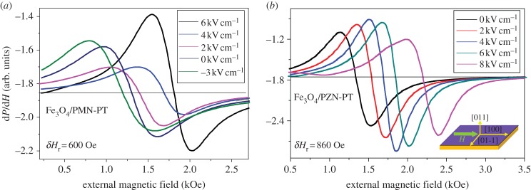
E-field tuning of ferromagnetic resonance spectra in (a) Fe3O4/PMN-PT(011) and (b) Fe3O4/PZN-PT(011) structures, where external magnetic fields are applied along the in-plane [100] direction, and external electric fields are applied in the out-of-plane [011] direction. dP/dH represents the magnetic field derivative of microwave power absorption. (Online version in colour.)
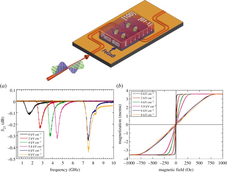
In addition to electrical control of microwave performance in ferrite/ferroelectric heterostructures, metallic/ferroelectric microwave heterostructures also have been studied. Most recently, we reported a new class of microwave magnetic thin-film materials, FeGaB films, which have large magnetostriction constant and low saturation fields desired for multiferroic composite applications [38]. With changing the B doping level, amorphous phase FeGaB was produced and led to excellent magnetic softness with coercivity less than 1 Oe, narrow FMR linewidth of 16–20 Oe at X-band (9.6 GHz), large λs of 50–70 ppm, high saturation magnetization of 11–15 kG, and a self-biased FMR frequency of 1.85 GHz. The combination of these properties makes the FeGaB films potential candidates for tunable ME microwave devices and other RF/microwave magnetic device applications. In our work, amorphous 100 nm thick FeGaB films were co-sputtered on single-crystal PZN-PT(011) substrates at room temperature. A magnetic easy axis along the in-plane [01-1] direction was made as an external magnetic field of 100 Oe was applied along this direction during the film growth. An Au layer was deposited on the back side of the PZN-PT substrate as the bottom electrode. The sample was laid face down on a coplane waveguide with two ports connected to a network analyser as schematically shown in figure 2. Electric fields were applied perpendicularly to the substrates, and microwave propagation direction was along the magnetic easy axis [01-1]. E-field manipulation of microwave performance in FeGaB/PZN-PT was measured by the network analyser in the manner of sweeping frequency. Figure 2a shows electrical tuning of transmission coefficients S21, defined as forward voltage gain, in FeGaB/PZN-PT(011) structures. Upon increasing the voltage, the absorption peak position, representing the FMR frequency, exhibits strong electric field dependence [33]. The lowest FMR frequency is 1.75 GHz at zero electric field, and the highest is 7.57 GHz at 6 or 8 kV cm−1. The total electrostatically tunable FMR frequency range is 5.82 GHz which is about two orders of magnitude higher than other reported values [35]. This large enhancement in resonance frequency upon applying electric fields also can be interpreted by equations (2.1) and (2.2). A positive Heff along the in-plane [01-1] direction was produced as a result of the positive magnetostriction of FeGaB and E-field-induced tensile strain (positive d) in PZN-PT(011). Therefore, the resonance frequency f is driven to high-frequency region as described in equation (2.1), where the external magnetic field is a constant. Figure 2b shows the E-field dependence of magnetic hysteresis loops as the magnetic field was applied along the [100] direction. The magnetization process turns out to be harder and shows a large change in magnetization saturation field from 10 to 700 Oe as the electric field was applied from 0 to 6 kV cm−1. This is mainly due the large positive magnetostriction of FeGaB and the E-field-induced compressive strain along [100] direction, which results in a large negative Heff and magnetic hard axis along this direction.
Figure 2.
(a) E-field dependence of microwave transmission absorption, S21, with frequency sweeping. The electric field was applied in the out-of-plane [011] direction; microwave propagation direction was along the in-plane [01-1] direction. The absorption peak represents the FMR frequency. (b) E-field dependence of magnetic hysteresis loops, where the magnetic field was applied along the [100] direction. (Online version in colour.)
We have demonstrated strong ME couplings in ferrite/ferroelectric and magnetic metal/ferroelectric heterostructures, which can be used to control microwave performance and realize tunable RF devices. We also made many other multiferroic heterostructures in our laboratory for different applications. A summary of the ME coupling of them is shown in table 1. The largest E-field-induced Heff of 3500 Oe was achieved in terfenol-D/PZN-PT(011) structure owing to the enormous magnetostriction constant in the magnetic phase. The giant electrostatically tunable magnetic anisotropy as well as FMR frequency makes these multiferroic heterostructures great candidates for reconfigurable microwave multiferroic devices with ultra-low power.
Table 1.
The comparison of ME coupling in various multiferroic heterostructures. YIG, yttrium iron garnet ferrite.
| structure | δH (Oe) | δH/δE (Oe cm kV−1) | δf (MHz) | δf/δE (MHz cm kV−1) |
|---|---|---|---|---|
| YIG/PZN-PT | — | — | 220 | 35 |
| Ni2MnGa/PMN-PT | 230 | 41 | — | — |
| FeCoB/PZN-PT | 500 | 82 | 4300 | 720 |
| NiFe (10 nm)/PZN-PT | 150 | 25 | ||
| NiCo/PZN-PT | 400 | 65 | ||
| FeGaB/PMN-PT | 330 | 33 | — | — |
| FeGaB/PZN-PT | 750 | 94 | 5820 | 970 |
| NZFO/PMN-PT | 50 | 8 | — | — |
| ZFO/PMN-PT | 140 | 23 | — | — |
| Fe3O4/PMN-PT | 600 | 67 | — | — |
| Fe3O4/PZN-PT | 860 | 108 | — | — |
| terfenol-D/PZN-PT | 3500 | 590 |
3. Electrical tuning of magnetoresistance in layered multiferroic heterostructures for ultra-low power electronics
An energy-efficient approach to electrically modulating magnetoresistance has been demonstrated in multiferroic AMR and GMR heterostructures. A giant E-field-induced magnetic anisotropy caused by a strong ME coupling is used to control the orientation of magnetization and thus dynamically manipulate magnetoresistance in AMR and GMR devices [32,34]. This can be expressed in the equation of the resistance as a function of Heff:
 |
3.1 |
Here, Hk and Hd are magnetic anisotropy field and demagnetization field which are quite small in soft magnetic thin films, and θ is the angle between the magnetization and the current flow which highly depends on the external magnetic field H and Heff. Figure 3 shows E-field modulating magnetoresistance in a multiferroic AMR structure of Ni80Co20/PZN-PT(011), where 40 nm thick Ni80Co20 films with λs=−20 ppm were deposited on (011)-oriented single crystal PZN-PT(011) substrates by magnetron sputtering. A magnetic easy axis along the in-plane [01-1] direction was made as the sample was in the presence of a magnetic field of 200 Oe during the deposition. The current and applied external magnetic fields are both parallel to the in-plane [100] direction (magnetic hard axis). Without a magnetic bias field, a minimum AMR was achieved at zero E-field caused by the orthogonality between the magnetization direction (easy axis) and the electric current (hard axis) as schematically shown in figure 3a. On increasing the strength of the E-field, which is applied in the out-of-plane [011] direction, the orientation of the magnetization is rotated in-plane from [01-1] to [100] and parallel to the current direction, therefore resulting in the maximum magnetoresistance according to equation (3.1). The magnetization rotation is due to the large electric-field-induced positive Heff (λs<0, d<0,λsd>0) that changes the magnetic easy axis to the [100] direction. Similar results were observed when an external magnetic bias field of 50 Oe was applied along [01-1] direction, in which a large electric-field-induced magnetic anisotropy is required to firstly overcome external magnetic bias field and then rotate magnetic moments to [100] direction and yield the maximum magnetoresistance. E-field dynamic tuning of magnetoresistance was also demonstrated as shown in figure 3b. Without magnetic bias fields, magnetoresistance was well modulated with a square wave electric field (0–2 kV cm−1) at a frequency of 0.5 Hz. Under a magnetic bias field of 50 Oe, magnetoresistance was periodically changed with a sine wave E-field (1–4 kV cm−1) [34].
Figure 3.
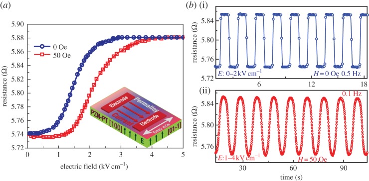
(a) E-field modulation of AMR in Ni80Co20/PZN-PT(011) with magnetic bias fields of 0 and 50 Oe, where the initial magnetic easy axis is along [01-1] direction and perpendicular to the measured current and external magnetic fields. (b) E-field dynamically modulating AMR under various external magnetic bias fields of 0 (i) and 50 Oe (ii) as a response to square wave and sine wave E-fields, respectively. (Online version in colour.)
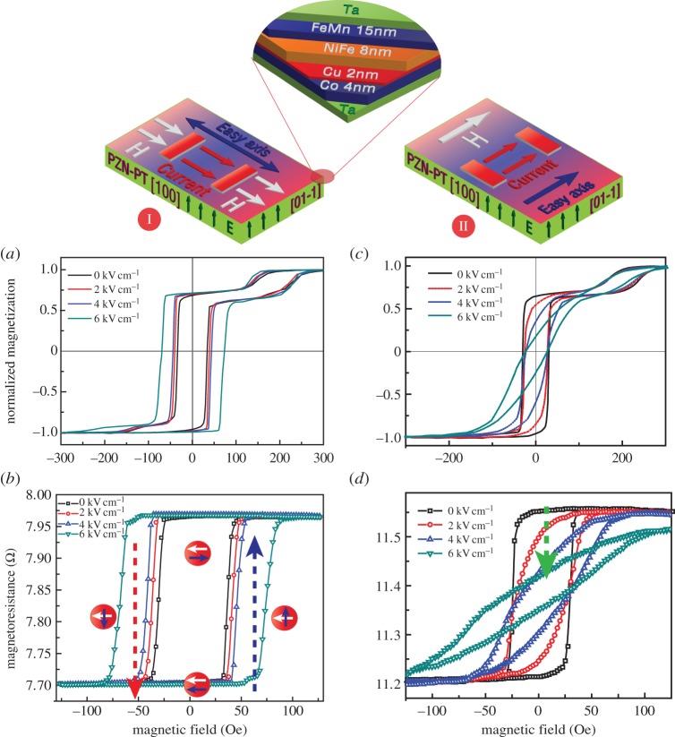
In addition, spin valves or GMR structures of Ta(10 nm)/FeMn(15 nm)/Ni80Fe20(8 nm)/Cu(2 nm)/Co(4 nm)/Ta(10 nm) were directly deposited onto (011)-oriented PZN-PT substrates without vacuum by magnetron sputtering as schematically shown in figure 4. Here, Co is the free layer which has a negative magnetostriction constant of −50 ppm; Ni80Fe20 is the pinned magnetic layer with near-zero magnetostriction constant. During the deposition, a magnetic easy axis along [100] (configuration I) or [01-1] (configuration II) was produced with the assistance of an external magnetic field. Figure 4a,c shows the E-field dependence of magnetic hysteresis loops in the two measurement configurations, where the magnetic easy axis, current direction as well as the external magnetic field are parallel to [100] direction (I; figure 4a) and [01-1] direction (II; figure 4c). As E-field increases, the changes in magnetic hysteresis loops exhibit an opposite trend in both configurations, indicating that the electric-field-induced magnetic anisotropy results in a magnetic easy axis along [100] direction and hard axis along [01-1] direction. In addition, the coercive field was significantly enhanced by 100% in configuration I as an E-field of 6 kV cm−1 was applied. For pinned magnetic layer of Ni80Fe20, the hysteresis loops were barely changed under various E-fields owing to the near-zero magnetostriction constant [34].
Figure 4.
E-field dependence of magnetic hysteresis loops (a,c) and giant magnetoresistance (b,d) in multiferroic structure of FeMn/Ni80Fe20/Cu/Co/PZN-PT(011). The magnetic easy axis, current direction and external magnetic field are along [100] and [01-1] directions, respectively. (Online version in colour.)
Figure 4b,d shows the E-field modulation of GMR for both configurations. Typical magnetoresistance hysteresis loops with a GMR ratio of 3% were achieved for configuration I (figure 4b). The coercive field was found to increase by 100% upon applying an electric field of 6 kV cm−1, which could enable a 180° magnetization switching in Co layer as illustrated by the arrow lines. By taking advantage of this, magnetoresistance switching up to 3% was achieved by reducing the electric field under various magnetic fields of 55 Oe or −55 Oe. In configuration II, E-field dependence of magnetoresistance shows similar hysteresis loops to those observed in the magnetization process (figure 4c). We related this phenomenon to the E-field-induced magnetic anisotropy field, which leads to a maximum 90° magnetization rotation. However, only half the GMR ratio was achieved in this configuration because of an E-field-induced 90° magnetization rotation rather than 180° magnetization switching. This result was different from the GMR change in configuration I, where a 180° magnetization switching takes place owing to the E-field tuning of coercive field, which results in the maximum resistance change of 3%.
4. E-field control of exchange bias in antiferromagnetic/ferromagnetic/ferroelectric multiferroic heterostructures
We have demonstrated previously that strain-mediated ME coupling in multiferroic composites leads to an E-field-induced magnetic anisotropy that results in a change in FMR and magnetoresistance. It can be used for tunable spintronics and microwave devices. However, in information storage systems, such as MERAMs, a 180° deterministic magnetization switching is required. It has been reported in exchange-coupled multiferroic systems that the ferromagnetic order is switchable by changing its neighboured antiferromagnetic orders. For example, Borisov et al. [39] demonstrated in 2005 that the perpendicular exchange bias field of the ME heterostructure [Co/Pt]×3]/Cr2O3(111) can be controlled by E-field and magnetic field cooling. In addition, E-field-induced exchange bias shift in multiferroic NiFe/YMnO3 heterostructures which resulted in one-way magnetization switching was also demonstrated at very low temperatures by Laukhin et al. [40]. Here, we show E-field-modulated exchange bias and realization of near 180° dynamic magnetization switching at room temperature in novel antiferromagnetic (AFM)/ferromagnetic (FM)/ferroelectric (FE) multiferroic heterostructures of FeMn/Ni80Fe20/FeGaB/PZN-PT(011). The E-field tuning of exchange bias and near 180° deterministic magnetization switching at room temperature in AFM/FM/FE multiferroic heterostructures pave a new way for MERAMs and other memory technologies [25].
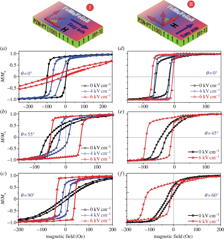
In our work, exchange-coupled films of Ta(5 nm)/FeMn(15 nm)/Ni80Fe20(2 nm)/FeGaB(14 nm)/Ta(20 nm) were deposited onto (011) cut single-crystal FE PZN-PT(011) substrates using magnetron sputtering. Amorphous FeGaB film with a large magnetostriction constant of 70 ppm was selected as the FM phase [38]. A (111)-oriented FeMn film was deposited as the AFM layer, which was facilitated by inserting a 2 nm thick Ni80Fe20 layer between FeGaB and FeMn to induce a strong exchange coupling in the FeMn/Ni80Fe20/FeGaB multilayer. The FeGaB film was deposited in the presence of a magnetic field, which led to an in-plane magnetic easy axis either along the in-plane [100] (d31) (configuration I) or [01-1] (d32) of PZN-PT (configuration II). Figure 5 presents the E-field dependence of magnetic hysteresis loops for both configurations. At zero E-field, an exchange bias field of 48 Oe was observed in the magnetic hysteresis loop for configuration I at θ=0° (figure 5a). On applying electric fields through the thickness direction of the PZN-PT(011) substrate, the magnetization of FeGaB turns out to be hard to saturate. This mainly arises for the E-field-induced negative Heff in the [100] direction. A slight reduction in exchange bias of ΔHex=−4 Oe was also observed. As an external magnetic field was applied along θ=55°, a much more pronounced E-field dependence of exchange bias was observed, exhibiting a remarkable downwards shift of the exchange bias from 45 to 3 Oe at an applied E-field of 6 kV cm−1, as shown in figure 5b. At θ=90°, the magnetic hysteresis loops turn to a square shape due to the E-field-induced positive effective magnetic anisotropy along [01-1] direction, which was accompanied with a negligible change in the exchange bias field. In configuration II, an opposite trend of magnetic hysteresis loops and exchange bias shifts is observed at varying E-fields. An E-field-induced magnetic field along the magnetic easy axis was achieved without notable variation of exchange bias fields for θ=0°, as shown in figure 5d. However, for θ=45° and 60°, significant enhancements of Hex from 33 to 50 Oe and from 22 to 70 Oe with ΔHex/Hex=218% were achieved respectively as illustrated in figure 5e,f.
Figure 5.
(a–c) E-field dependence of magnetic hysteresis loops in configuration I for θ=0°, 55°, 90°. (d–f) E-field dependence of magnetic hysteresis loops in configuration II for θ=0°, 45°, 60°. (Online version in colour.)
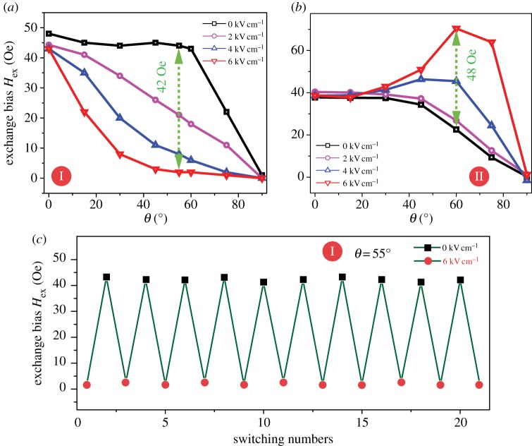
Figure 6 displays the angular dependence of exchange bias Hex under various E-fields for both configurations I and II. A strong θ angle dependence of the exchange bias Hex on E-field was observed at intermediate θ angles between 0° and 90°. A maximum E-field-induced exchange field change of ΔHex=−42 Oe was observed at θ=55° for configuration I, as shown in figure 6a, whereas a significant enhancement of ΔHex up to 48 Oe was achieved, as shown in figure 6b, for configuration II. To further confirm the repeatability of exchange-bias field shift under various E-fields, exchange-bias field versus switching number of E-field is shown in figure 6c at 0 and 6 kV cm−1, indicating a robust and repeatable E-field-induced exchange-bias shift.
Figure 6.
Angular dependence of exchange bias under various E-fields. (a) Correlation of exchange bias with E-field in configuration I. Arrow line indicates a remarkable E-field-induced exchange bias downwards shift up to 42 Oe at θ=55°. (b) Correlation of exchange bias with E-field in configuration II. Arrow line displays a significant E-field-induced exchange bias upwards shift up to 48 Oe or 218% at θ=60°. (c) Exchange-bias field versus switching number of E-fields between 6 (circles) and 0 kV cm−1 (squares). (Online version in colour.)
The giant E-field dependence of exchange bias in AFM/FM/FE heterostructures provides great opportunities for realizing electrically deterministic magnetization switching in FeGaB film, which constitutes one important step towards MERAMs, and has great potential in E-field writing of novel spintronics and memory devices [25].
5. Electrical non-volatile tuning of magnetic states in layered multiferroic heterostructures
Magnetization non-volatile switching is of great fundamental importance for spintronic devices and information storage systems. Conventionally, it is realized by applying magnetic fields which are produced by large electric currents, or more recently with the spin torque effect by passing a spin polarized current through a magnetic film. Both methods require large current or current density, which make the system bulky, noisy and consuming a lot of energy. Therefore, an energy-efficient way of voltage- or electric field-induced non-volatile magnetization switching has attracted a lot interest in the past decade. It is well known that electric-field-induced phase transitions are very prominent in ferroelectric materials with compositions near the morphotropic phase boundary. For example, a rhombohedral-to-orthorhombic phase transition takes place in (011)-oriented PZN(6–7%)-PT under sufficient poling fields. Most of such phase transitions are non-volatile, where extra energy is required to overcome remnant states to return to initial states. Therefore, it is expected to display a hysteresis-type lattice change as a function of E-field. This effect can be used for realizing non-volatile spintronics and microwave devices based on multiferroic heterostructures.
In our work, we deposited 50 nm thick FeGaB films on (011)-oriented PZN-PT substrates. The electric field was applied in the out-of-plane [011] direction, whereas the external magnetic field was applied along [01-1] direction. FMR spectra of FeGaB films were measured in field-sweeping and frequency-sweeping modes. A positive Heff is expected due to the positive magnetostriction of FeGaB and E-field-induced tensile strain along [01-1] direction, which could drive FMR to high-frequency region or to low magnetic field region in frequency- or field-sweeping mode, respectively. Figure 7 shows hysteresis loops of FMR field versus E-field with a working frequency of 12 GHz and FMR frequency versus E-field with a magnetic bias field of 50 Oe. Both of them exhibit a linear correlation at low electric fields, indicating no ferroelectric phase change taking place in PZN-PT(011). As the electric field reaches a critical threshold of Ec1∼5.8 kV cm−1, sudden changes in both resonance field and frequency are observed, suggesting the appearance of phase transition with a drastic lattice change and giant ME coupling effect. At high electric field, FMR field and frequency saturate with little strain variation. On reducing E-field from 8 kV cm−1, the orthorhombic phase and strain state remains fairly stable until another critical field of Ec2∼3 kV cm−1 is reached. Symmetric behaviour occurs when applying a negative E-field from 0 to −8 kV cm−1. Such hysteretic type of E-field control of strain and magnetic states provides an opportunity to realize non-volatile FMR switching, which is extremely important in reconfigurable ME microwave devices.
Figure 7.
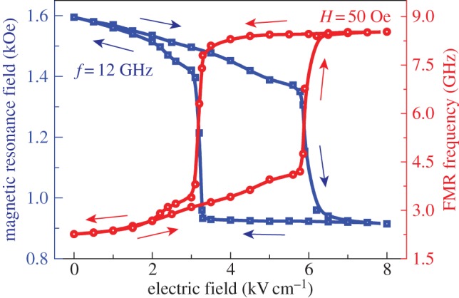
Hysteresis loops of E-field versus FMR frequency measured under a bias magnetic field of 50 Oe (circles) and E-field versus FMR field with working frequency of 12 GHz (squares) in FeGaB/PZN-PT(011) heterostructures. The electric field was applied in the out-of-plane [011] direction, and the magnetic field was applied in-plane along [01-1] direction. (Online version in colour.)
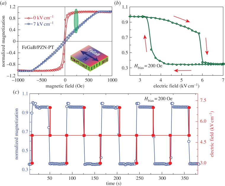
E-field tuning of magnetization and non-volatile magnetization switching in FeGaB/PZN-PT(011) is shown in figure 8. The change in normalized magnetic hysteresis loops of FeGaB/PZN-PT(011) at various electric fields (figure 8a) implies that a large E-field-induced negative Heff is produced which makes the magnetization saturation harder in the [100] direction. As an external magnetic bias of 200 Oe was applied along the [100] direction, a hysteresis loop of the magnetization as a function of the electric field was observed as shown in figure 8b, which is consistent with the E-field-induced FMR hysteresis loops in figure 7. This indicates that reversible and stable lattice change owing to the phase transition in PZN-PT takes place, which results in two remnant magnetization states. Voltage-impulse non-volatile switching of magnetization between two remnant magnetization states is demonstrated in figure 8c. An electric field of 5 kV cm−1 is applied as a bias. Field impulses (less than 1 s) of 3 and 7 kV cm−1 are applied alternately at a period of 75 s. As an E-field impulse of 3 kV cm−1 is applied, magnetization in FeGaB rises and remains at a high magnetization ratio of 95%. By contrast, the magnetization ratio is reduced and stays at 35% as an E-field impulse of 7 kV cm−1 is applied. Therefore, dynamic E-field-impulse-induced magnetization switching in FeGaB was realized. This memory type of magnetization switching would result in non-volatile FMR tuning with great energy efficiency.
Figure 8.
(a) E-field dependence of magnetic hysteresis loops of FeGaB/PZN-PT(011), where the magnetic field is along [100] direction. (b) Hysteresis loop of magnetization versus E-field of FeGaB under a magnetic bias field of 200 Oe, when the PZN-PT substrate undergoes phase transition. (c) E-field impulse-induced non-volatile magnetization switching. (Online version in colour.)
6. Summary
Electric field control of magnetic states, including magnetic anisotropy, FMR, magnetoresistance, exchange bias, as well as non-volatile magnetization switching, has been successfully demonstrated in multiferroic heterostructures. Giant FMR field- and frequency-tunable range with small linewidth observed in metal ferromagnetic/ferroelectric and spin–spray-deposited ferrite/ferroelectric heterostructures shows great opportunities for the next generation of electrostatically tunable microwave devices, such as filters, phase shifters, resonators, etc. In tunable multiferroic magnetoresistance devices, the resistance was modulated depending upon electrically rotating the magnetization directions by applying voltage rather than by applying magnetic field or current. This concept and design satisfies the ever increasing demands for faster, smaller and ultra-low power electronics and has a great impact on the magnetoresistance devices research area. In exchange-coupled multiferroic heterostructures, 180° deterministic magnetization switching in ferromagnetic layers has been realized through electrically tuning the exchange coupling. This electric-field-induced 180° deterministic magnetization switching is essential for MERAMs, where magnetic bits are switched by electric field. Some preliminary results on electrically induced non-volatile magnetization switching are also presented in this review, in which a voltage impulse can switch magnetization parentally. In a word, the effects of voltage-tuning magnetic states in multiferroic heterostructures are found to be extremely significant, which show great potential for delivering smaller, faster, ultra-low power electronic- and microwave-tunable devices.
Funding statements
This work is financially supported by AFRL through UES FA8650-090-D-5037, NSF under award nos. 0746810 and 0824008.
References
- 1.Eerenstein W, Mathur ND, Scott JF. 2006. Multiferroic and magnetoelectric materials. Nature 442, 759–765. ( 10.1038/nature05023) [DOI] [PubMed] [Google Scholar]
- 2.Ramesh R, Spaldin NA. 2007. Multiferroics: progress and prospects in thin films. Nat. Mater. 6, 21–29. ( 10.1038/nmat1805) [DOI] [PubMed] [Google Scholar]
- 3.Weisheit M, Fahler S, Marty A, Souche Y, Poinsignon C, Givord D. 2007. Electric field-induced modification of magnetism in thin-film ferromagnets. Science 315, 349–351. ( 10.1126/science.1136629) [DOI] [PubMed] [Google Scholar]
- 4.Wang J, et al. 2003. Epitaxial BiFeO3 multiferroic thin film heterostructures. Science 299, 1719–1722. ( 10.1126/science.1080615) [DOI] [PubMed] [Google Scholar]
- 5.Tsymbal EY, Kohlstedt H. 2006. Applied physics: tunneling across a ferroelectric. Science 313, 181–183. ( 10.1126/science.1126230) [DOI] [PubMed] [Google Scholar]
- 6.Eerenstein W, Wiora M, Prieto JL, Scott JF, Mathur ND. 2007. Giant sharp and persistent converse magnetoelectric effects in multiferroic epitaxial heterostructures. Nat. Mater. 6, 348–351. ( 10.1038/nmat1886) [DOI] [PubMed] [Google Scholar]
- 7.Bibes M, Barthelemy A. 2008. Multiferroics: towards a magnetoelectric memory. Nat. Mater. 7, 425–426. ( 10.1038/nmat2189) [DOI] [PubMed] [Google Scholar]
- 8.Srinivasan G. 2010. Magnetoelectric composites. Annu. Rev. Mater. Res. 40, 153–178. ( 10.1146/annurev-matsci-070909-104459) [DOI] [Google Scholar]
- 9.Ohno H. 2010. A window on the future of spintronics. Nat. Mater. 9, 952–954. ( 10.1038/nmat2913) [DOI] [PubMed] [Google Scholar]
- 10.Spaldin NA, Cheong SW, Ramesh R. 2010. Multiferroics: past, present, and future. Phys. Today 63, 38–43. ( 10.1063/1.3502547) [DOI] [Google Scholar]
- 11.Hu J-M, Li Z, Chen L-Q, Nan C-W. 2011. High-density magnetoresistive random access memory operating at ultralow voltage at room temperature. Nat. Commun. 2, 553 ( 10.1038/ncomms1564) [DOI] [PMC free article] [PubMed] [Google Scholar]
- 12.Liu M, et al. 2009. Giant electric field tuning of magnetic properties in multiferroic ferrite/ferroelectric heterostructures. Adv. Funct. Mater. 19, 1826–1831. ( 10.1002/adfm.200801907) [DOI] [Google Scholar]
- 13.Lou J, Reed D, Liu M, Pettiford C, Sun NX. 2009. Novel electrostatically tunable FeGaB/(Si)/PMN-PT multiferroic heterostructures for microwave application. In IEEE MTTS Int. Microwave Symp. Digest 2009, pp. 33–36. New York, NY: IEEE; ( 10.1109/MWSYM.2009.5165625) [DOI] [Google Scholar]
- 14.Ma J, Hu JM, Li Z, Nan CW. 2011. Recent progress in multiferroic magnetoelectric composites: from bulk to thin films. Adv. Mater. 23, 1062–1087. ( 10.1002/adma.201003636) [DOI] [PubMed] [Google Scholar]
- 15.Nan CW, Bichurin MI, Dong SX, Viehland D, Srinivasan G. 2008. Multiferroic magnetoelectric composites: historical perspective, status, and future directions. J. Appl. Phys. 103, 031101 ( 10.1063/1.2836410) [DOI] [Google Scholar]
- 16.Scott JF. 2007. Data storage. Multiferroic memories. Nat. Mater. 6, 256–257. ( 10.1038/nmat1868) [DOI] [PubMed] [Google Scholar]
- 17.Srinivasan G, Fetisov YK. 2006. Ferrite-piezoelectric layered structures: microwave magnetoelectric effects and electric field tunable devices. Ferroelectrics 342, 65–71. ( 10.1080/00150190600946195) [DOI] [Google Scholar]
- 18.Das J, Song YY, Mo N, Krivosik P, Patton CE. 2009. Electric-field-tunable low loss multiferroic ferrimagnetic–ferroelectric heterostructures. Adv. Mater. 21, 2045–2049. ( 10.1002/adma.200803376) [DOI] [Google Scholar]
- 19.Chu YH, et al. 2008. Electric-field control of local ferromagnetism using a magnetoelectric multiferroic. Nat. Mater. 7, 478–482. ( 10.1038/nmat2184) [DOI] [PubMed] [Google Scholar]
- 20.Zhao P, Zhao ZL, Hunter D, Suchoski R, Gao C, Mathews S, Wuttig M, Takeuchi I. 2009. Fabrication and characterization of all-thin-film magnetoelectric sensors. Appl. Phys. Lett. 94, 243507 ( 10.1063/1.3157281) [DOI] [Google Scholar]
- 21.Dong SX, Zhai JY, Li JF, Viehland D. 2006. Small DC magnetic field response of magnetoelectric laminate composites. Appl. Phys. Lett. 88, 082907 ( 10.1063/1.2178582) [DOI] [Google Scholar]
- 22.Hu J-M, Nan CW. 2009. Electric-field-induced magnetic easy-axis reorientation in ferromagnetic/ferroelectric layered heterostructures. Phys. Rev. B 80, 224416 ( 10.1103/PhysRevB.80.224416) [DOI] [Google Scholar]
- 23.Li N, Liu M, Zhou Z, Sun NX, Murthy DVB, Srinivasan G, Klein TM, Petrov VM, Gupta A. 2011. Electrostatic tuning of ferromagnetic resonance and magnetoelectric interactions in ferrite-piezoelectric heterostructures grown by chemical vapor deposition. Appl. Phys. Lett. 99, 192502 ( 10.1063/1.3658900) [DOI] [Google Scholar]
- 24.Li Z, Wang J, Lin YH, Nan CW. 2010. A magnetoelectric memory cell with coercivity state as writing data bit. Appl. Phys. Lett. 96, 162505 ( 10.1063/1.3405722) [DOI] [Google Scholar]
- 25.Liu M, Lou J, Li SD, Sun NX. 2011. E-field control of exchange bias and deterministic magnetization switching in AFM/FM/FE multiferroic heterostructures. Adv. Funct. Mater. 21, 2593–2598. ( 10.1002/adfm.201002485) [DOI] [Google Scholar]
- 26.Zheng RK, Wang Y, Chan HLW, Choy CL, Luo HS. 2008. Substrate-induced strain effect in La0.875Ba0.125MnO3 thin films grown on ferroelectric single-crystal substrates. Appl. Phys. Lett. 92, 082908 ( 10.1063/1.2870100) [DOI] [Google Scholar]
- 27.Liu M, Obi O, Cai ZH, Lou J, Yang GM, Ziemer KS, Sun NX. 2010. Electrical tuning of magnetism in Fe3O4/PZN-PT multiferroic heterostructures derived by reactive magnetron sputtering. J. Appl. Phys. 107, 073916 ( 10.1063/1.3354104) [DOI] [Google Scholar]
- 28.Zheng RK, Jiang Y, Wang Y, Chan HLW, Choy CL, Luo HS. 2008. Investigation of substrate-induced strain effects in La0.7Ca0.15Sr0.15MnO3 thin films using ferroelectric polarization and the converse piezoelectric effect. Appl. Phys. Lett. 93, 102904 ( 10.1063/1.2979688) [DOI] [Google Scholar]
- 29.Drabble JR, Whyte TD, Hooper RM. 1971. Electrical conductivity of magnetite at low temperatures. Solid State Commun. 9, 275–278. ( 10.1016/0038-1098(71)90176-1) [DOI] [Google Scholar]
- 30.Liu J-M, Nan C-W. 2012. Ferroelectricity and multiferroicity: broader way to go beyond. Front. Phys. 7, 373–374. ( 10.1007/s11467-012-0257-9) [DOI] [Google Scholar]
- 31.Hu J-M, Li Z, Chen L-Q, Nan C-W. 2012. Design of a voltage-controlled magnetic random access memory based on anisotropic magnetoresistance in a single magnetic layer. Adv. Mater. 24, 2869–2873. ( 10.1002/adma.201201004) [DOI] [PubMed] [Google Scholar]
- 32.Liu M, Obi O, Lou J, Li SD, Xing X, Yang GM, Sun NX. 2011. Tunable magnetoresistance devices based on multiferroic heterostructures. J. Appl. Phys. 109, 07D913 ( 10.1063/1.3561771) [DOI] [Google Scholar]
- 33.Lou J, Liu M, Reed D, Ren YH, Sun NX. 2009. Giant electric field tuning of magnetism in novel multiferroic FeGaB/lead zinc niobate–lead titanate (PZN-PT) heterostructures. Adv. Mater. 21, 4711–4715. ( 10.1002/adma.200901131) [DOI] [Google Scholar]
- 34.Liu M, Li SD, Obi O, Lou J, Rand S, Sun NX. 2011. Electric field modulation of magnetoresistance in multiferroic heterostructures for ultralow power electronics. Appl. Phys. Lett. 98, 222509 ( 10.1063/1.3597796) [DOI] [Google Scholar]
- 35.Shastry S, Srinivasan G, Bichurin M, Petrov V, Tatarenko A. 2004. Microwave magnetoelectric effects in single crystal bilayers of yttrium iron garnet and lead magnesium niobate-lead titanate. Phys. Rev. B 70, 064416 ( 10.1103/PhysRevB.70.064416) [DOI] [Google Scholar]
- 36.Alivov Y, Morkoc H. 2009. Microwave ferrites, part 1: fundamental properties. J. Mater. Sci. 20, 789–834. ( 10.1007/s10854-009-9923-2) [DOI] [Google Scholar]
- 37.Liu M, Obi O, Lou J, Stoute S, Huang JY, Cai ZH, Ziemer KS, Sun NX. 2008. Spin-spray deposited multiferroic composite Ni0.23Fe2.77O4/Pb(Zr,Ti)O3 with strong interface adhesion. Appl. Phys. Lett. 92, 152504 ( 10.1063/1.2911743) [DOI] [Google Scholar]
- 38.Lou J, Insignares RE, Cai Z, Ziemer KS, Liu M, Sun NX. 2007. Soft magnetism, magnetostriction, and microwave properties of FeGaB thin films. Appl. Phys. Lett. 91, 182504 ( 10.1063/1.2804123) [DOI] [Google Scholar]
- 39.Borisov P, Hochstrat A, Chen X, Kleemann W, Binek C. 2005. Magnetoelectric switching of exchange bias. Phys. Rev. Lett. 94, 117203 ( 10.1103/PhysRevLett.94.117203) [DOI] [PubMed] [Google Scholar]
- 40.Laukhin V, et al. 2006. Electric-field control of exchange bias in multiferroic epitaxial heterostructures. Phys. Rev. Lett. 97, 227201 ( 10.1103/PhysRevLett.97.227201) [DOI] [PubMed] [Google Scholar]


