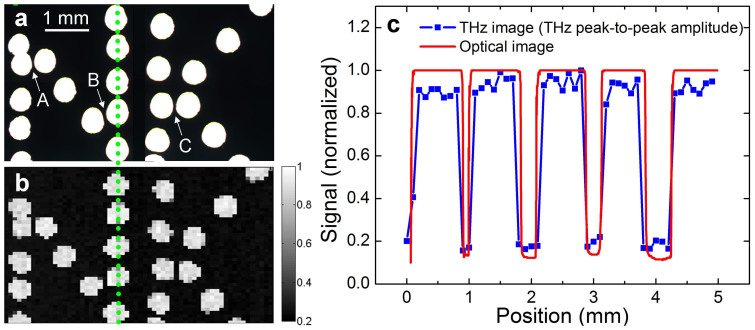
Figure 2. Comparing THz image and optical microscope image.
(a) Optical microscope image of multiple through-holes on PCB (printed circuit board) plate. Each hole is about 600 μm in size. Arrow A, B and C point at three hole pitches with characterized widths of about 60 μm, 80 μm and 75 μm, respectively. (b) THz image of multiple through-holes on PCB plate. (c) Spatial profiles of a series of representative holes retrieved from (a) and (b) along the green dotted line, as red line and blue solid squares, respectively.

