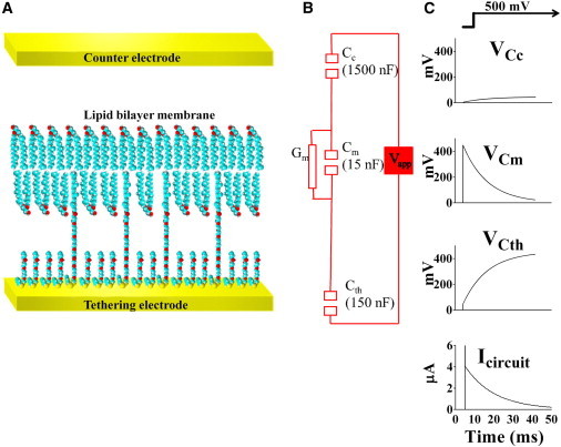
Figure 1.

(A) Schematic diagram of a typical tBLM used in these experiments. (B) The equivalent circuit for the tBLM used here. For the electrode area of 2.1 mm2, the actual values have been rounded to 1500 nF, 150 nF, and 15 nF to emphasize the 10-fold differences between the capacitances at each layer of the equivalent circuit. (C) Of the 500 mV step applied across the whole circuit, ∼1%, or 0.004504 V, is initially expressed across the gold counterelectrode, Cc, ∼10%, or 0.04504 V, across the tethering gold surface, Cth, and ∼90%, or 0.4504 V, across the tethered membrane, Cm. The current response (bottom plot) initially shows a capacitive spike due to charging of Cm, Cth, and Cc. After this initial spike, the current slowly decays due to the charge being redistributed across Cth and Cc. When Cth and Cc are fully charged, the voltage across the membrane and the current will have decayed to zero. To see this figure in color, go online.
