
Figure 1.
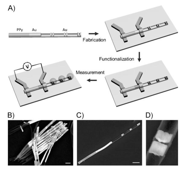
A) Schematic of the synthesis, device fabrication, surface functionalization, and measurement of hybrid PPy-rod/Au-rod/Au-disk-pair nanostructures. The Au–PPy nanorod portion is contacted with electrodes to form the electrical sensing elements, and the Au disks functionas SERS hotspots. The surface functionalization takes place over the entire exposed Au surface (disks and rods). B) An SEM image of assynthesized Au–Ni–Au–PPy nanorods. The Ni portions are subsequently removed by chemical etching to form the multigap structures (C). Scale bar = 1 μm. C) An SEM image of one PPy-rod/Au-rod/Au-disk-pair nanostructure made by OWL with a SiO2 backing layer. The structures consist of a PPy–Au rod segment (the PPy portion has a lower contrast than the Au portion) and three pairs of Au disks. Scale bar = 1 μm. D) Zoomed-in SEM image of a single pair of Au disks (disk thickness ≈120 nm, disk separation ≈30 nm).