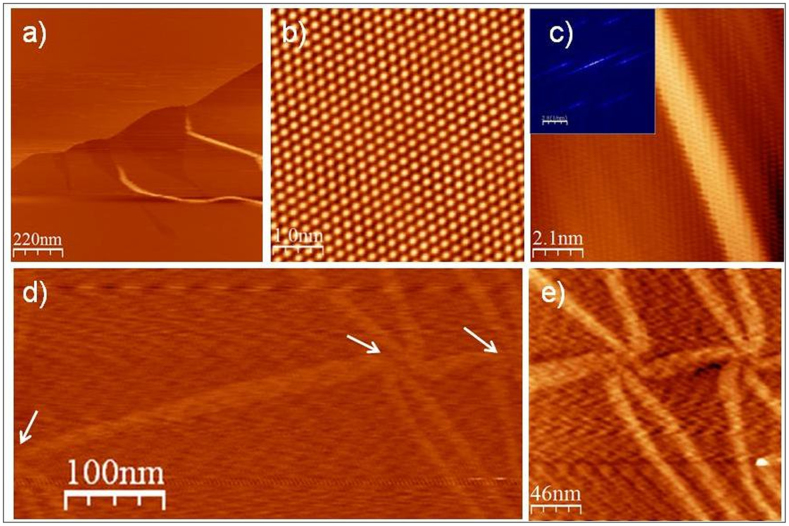
Figure 2. Morphology of trilayer graphene.
(a) Large STM image (−1.7 V, 1 nA) of trilayer graphene (b) Triangular type structures (5 × 5 nm2), (c) An STM image of corrugated graphene with nearly periodic ripples of nanometer wavelength (inset Fourier transform of the STM image) (d) STM image of three interconnected flower-shaped structures, (e) STM image of two interconnected flower-shaped domains. Vs = 0.05 V, It = 200 pA) for (b - e).

