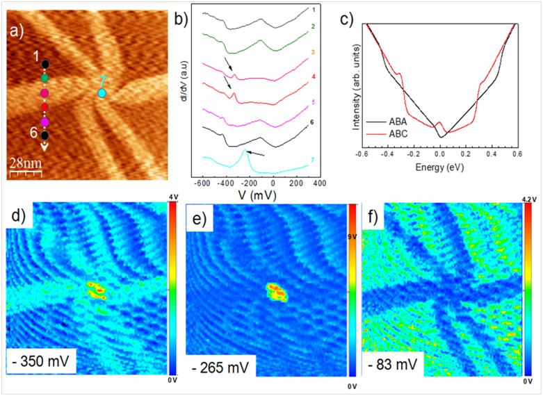
Figure 3. Flower-shaped domains on trilayer graphene.
(a) STM topography showing the flower-shaped domains (Vs = −0.05 V, It = 0.2 nA). (b) Spatially averaged dI/dV curves in five different regions of the graphene indicated in (a). The curves show two -resonance peaks located at −344.4 mV and −264.5 on wrinkles and in the middle of the wrinkles. (c) The calculated total density of states of ABA and ABC stacking; the LDOS of ABC stacking has an additional resonance peak located at the Dirac level in comparison with the LDOS of ABA stacking. (e–f) dI/dV maps at sample voltages −344.4 mV, −264.5 and −83.4 mV, respectively, showing the transition between graphene and flower-shaped domains. For all the images, the current was stabilized at the parameters in (a) and the feedback was then switched off. The maps were recorded using lock-in detection.

