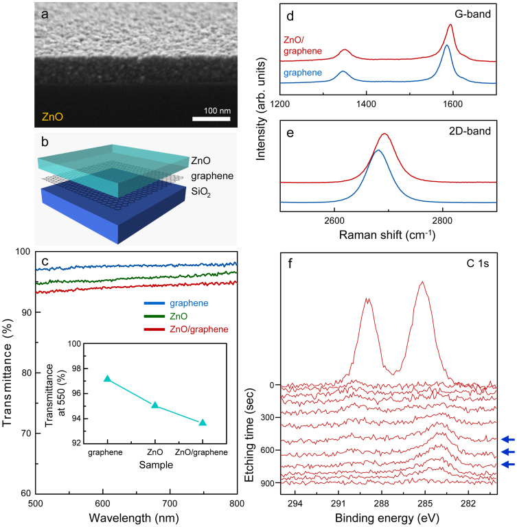
Figure 1.
(a) SEM image for solution-processed ZnO thin film on SiO2 (300 nm)/Si(001) substrate. (b) A schematic diagram of ZnO/graphene hybrid film. (c) Optical transmittance of graphene, ZnO, and ZnO/graphene. The inset compares the transmittance at 550 nm for different samples. (d) G-band and (e) 2D-band spectra with an excitation wavelength of 514 nm for graphene and ZnO/graphene hybrid film. (f) Evolution of the C 1s core level spectra of ZnO/graphene hybrid film as a function of etching time.

