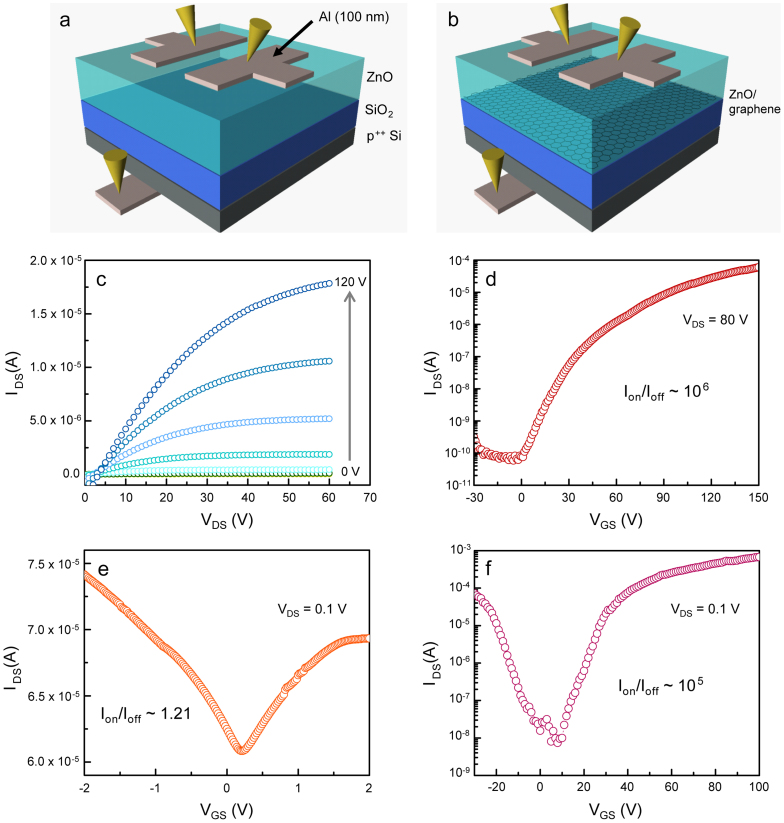
Figure 2.
Schematic illustration of the device structure, including the bottom-gate configuration, 300 nm-thick SiO2 gate dielectric, and 100 nm-thick Al source/drain contacts for (a) ZnO TFTs and (b) ZnO/graphene hybrid TFTs. (c) Output characteristic of ZnO TFTs at room temperature. Transfer characteristics of (d) ZnO TFTs, (e) electrochemically gate tuned graphene TFTs, and (f) ZnO/graphene TFTs.

