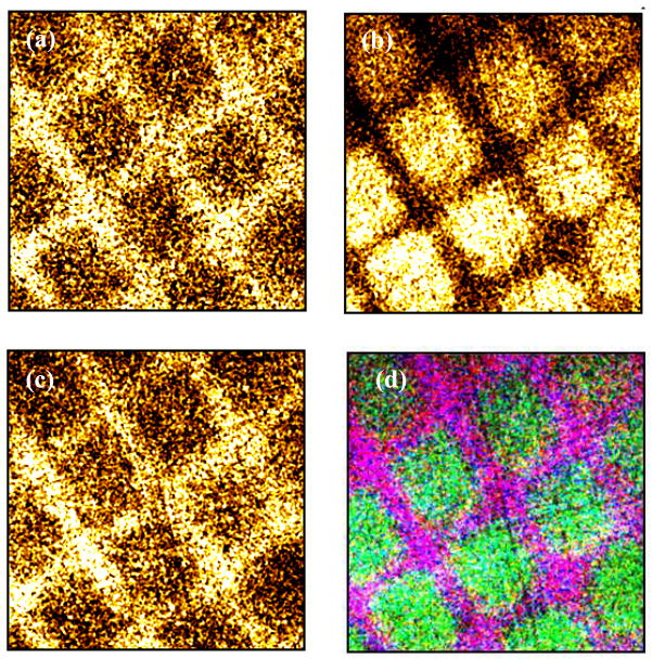
Figure 8.
XPS background corrected images of patterned graphene on a PFPA-functionalized silicon wafer: (a) F1s image, (b) C1s image, (c) Si2p image, (d) a superposition of all three elements (C: green, Si and F: purple). Image size: 400 μm × 400 μm. Spots marked i and ii are the areas selected for small spot analyses (see Table 4).

