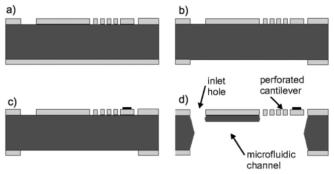
Figure 4.
Fabrication sequence for the SiN devices: (a) Patterning of perforated cantilevers in the SiN layer on the front side of the wafer. (b) Patterning of etch mask for microfluidic channel in the SiN layer on the back side of the wafer. (c) Patterning of metal pad at apex of the cantilever. (d) Definition of microchannel and release of the SiN devices in KOH.

