
Fig. 6.
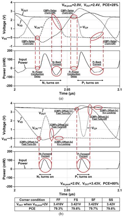
Simulation results of the active voltage doubler showing waveforms of the input/output voltages and input power with VIN,peak = 2 V, RLCL = 1 kΩ ∥ 2 nF, CIN = 2 nF, and fc = 13.56 MHz. (a) Without any offset-control functions. (b) With all three offset-control functions in the nominal and four process corner conditions.