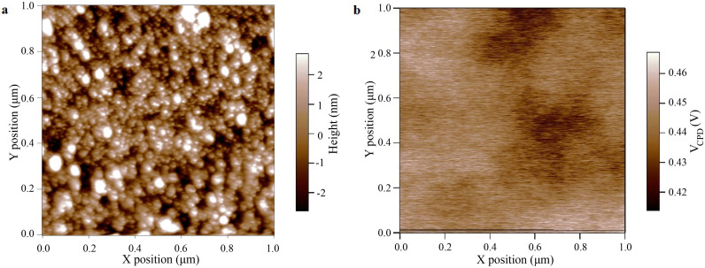
Figure 3.
(a) Atomic force microscopy topography image of a ZnO thin film deposited by RF sputtering. Small grains with dimensions of tens of nanometers can be observed (b) Two-dimensional contact potential difference VCPD image of the same surface imaged in Fig. 3a. The image is acquired at an equilibrium distance of 20 nm with an oscillation of 5 nm.

