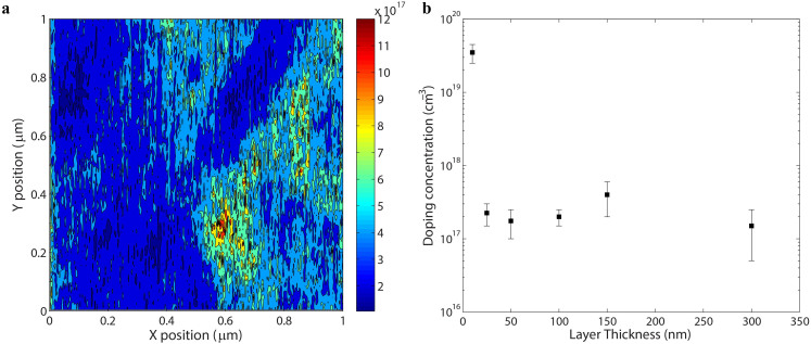
Figure 4.
(a) Two-dimensional map of the charge carrier density in a 150 nm thick ZnO film.(b) doping concentration versus layer thickness for a set of ZnO thin films (from 10 to 300 nm). All the samples are deposited under the same conditions (deposition rate 0.1 Å/sec, Ar pressure 0.8 mTorr). The effective doping concentration does not correlate with the layer thickness, except for the 10 nm layer. For each sample, three different regions have been scanned. The standard deviation of the value of the effective doping concentration is reported.

