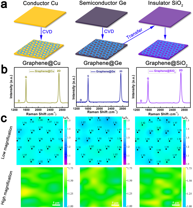
Figure 2.
(a) Schematic illustration for the fabrication of the testing graphene film samples, i.e., large-area monolayer graphene films on conductor Cu, semiconductor Ge and insulator SiO2 substrates; (b) Raman spectra of the graphene films on Cu, Ge and SiO2 substrates, respectively; (c) Raman mapping results of the monolayer graphene films on Cu, Ge and SiO2 substrates at both low and high magnification, showing the uniformity and the coverage of the as-grown monolayer graphene films on these substrates. The Raman mapping area at low magnification is 1 × 1 cm2, as illustrated in Supplementary Figure S4.

