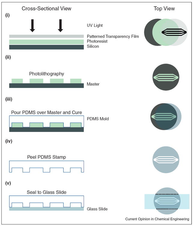
Figure 1.

Microfluidic device fabrication by soft lithography. Left panel shows cross-sectional view while the right panel displays a top down perspective of the fabrication process. (i) Microfluidic channel geometries can be designed on a computer program and printed to a high-resolution transparency film. (ii) After applying photoresist to a silicon wafer, the drawn geometry can be transferred as a ‘master’ mold via photolithography. (iii) Polydimethylsiloxane (PDMS), a soft elastomeric material, is poured over the master mold, cured and (iv) peeled off, retaining the geometric features. (iv) Finally the new PDMS mold can be sealed to a glass slide or coverslip, leaving open channels.
Adapted from [46].
