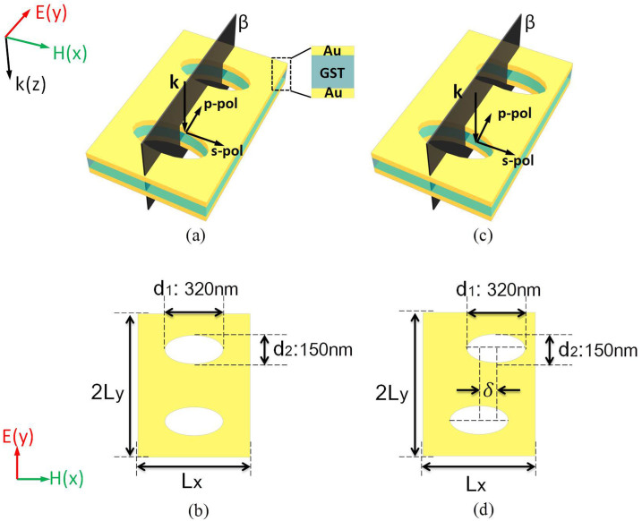
Figure 1.
(a) Schematic of the symmetric MDM-ENA(δ = 0 nm) consisting of a 160 nm thick Ge2Sb2Te5 dielectric layer between two 30 nm thick Au films perforated with a square array of elliptical holes suspended in a vacuum. (b) Illustration of the symmetric element of ENA, the lattice constants are Lx = 500 nm, Ly = 400 nm and hole diameters are d1 = 320 nm, d2 = 150 nm. (c) Schematic of the asymmetric MDM-ENA(δ = 70 nm) consisting of a 160 nm thick Ge2Sb2Te5 dielectric layer between two 30 nm thick Au films perforated with ENA suspended in a vacuum. (d) Illustration of the asymmetric element of ENA, the lattice constant is Lx = 500 nm, Ly = 400 nm, hole diameters are d1 = 320 nm, d2 = 150 nm, δ is the distance of the upper elliptical hole from the centre(δ = 70 nm).

