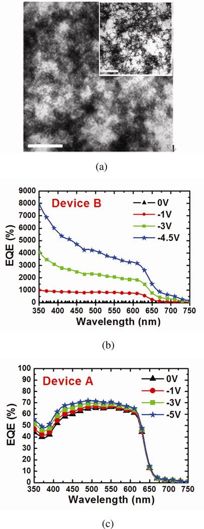
Figure 2. TEM images and external quantum efficiency.
(a) TEM images of P3HT:PCBM/CdTe NPs (~3.1% (31mg/mL)) film. Scale bar in the major image is 200 nm and is 1´m for the inset. The solution was drop cast on a TEM grid for sample preparation. Highly condensed aggregates of CdTe NPs are observed and thread-like features are clearly visible in the inset. (b) EQE of device B under zero and reverse bias. Higher than 100% EQE is obtained under reverse bias, even at the absorption edge of CdTe NPs (~700 nm). (c) EQE of device A measured under the same conditions.

