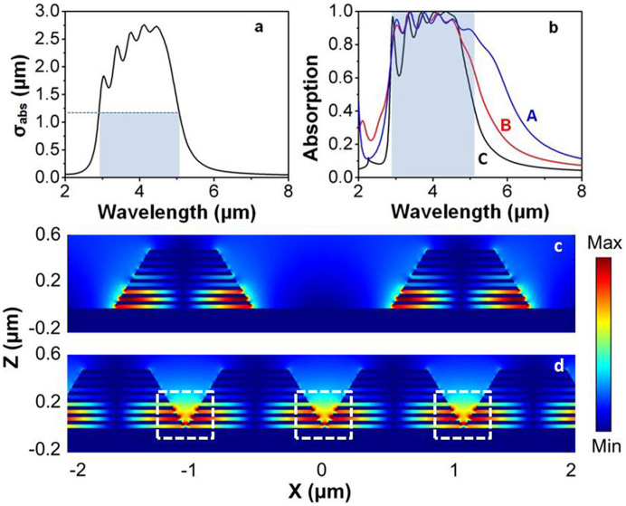
Figure 2. Period dependence of the HMM pattern array.
(a) 1D absorption cross-section of a single 8-pair HMM waveguide taper unit with the top and bottom widths of 550 nm and 1.14 μm, respectively. The thicknesses of the metal and dielectric films are both 35 nm, respectively. (b) Absorption spectra of three periodic patterns with the period of (A) 1.14 μm, (B) 1.35 μm and (C) 2.26 μm. (c) and (d) are modeled E-field distributions in (c) structure C and (d) structure A at the wavelength of 5.15 μm.

