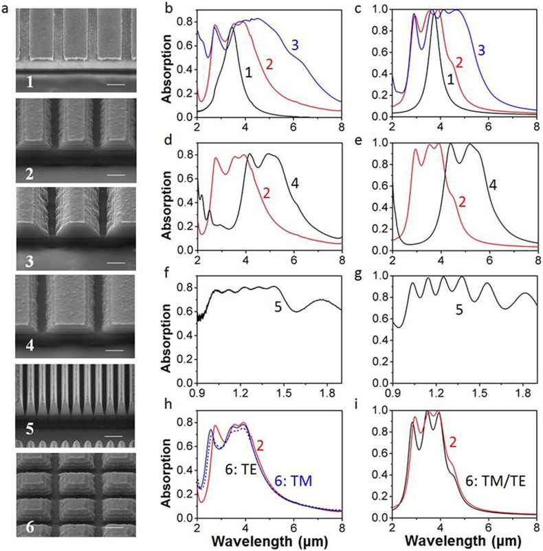
Figure 3. Multi-layered HMM waveguide taper array for broadband absorption engineering.
(a) 54°-tilted SEM images of 6 samples of super absorptive meta-films. The period and width of the top Ag pattern of sample 1 are 950 nm and 720 nm, respectively. For samples 2–6, the period, top width and bottom width parameters are (1.17 μm, 500 nm, 950 nm) for sample 2, (1.35 μm, 480 nm, 1.14 μm) for sample 3, (1.57 μm, 850 nm, 1.35 μm) for sample 4, (300 nm, 110 nm, 270 nm) for sample 5 and (1.17 μm, 500 nm, 950 nm) for sample 6, respectively. The scale bar is 500 nm. (b, d, f, h) and (c, e, g, h) show measured and modeled absorption spectra of these 6 samples (indicated by sample number), respectively.

