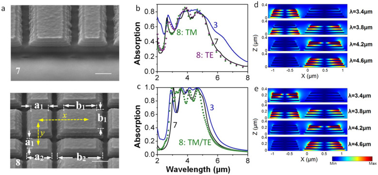
Figure 4. Multi-unit HMM waveguide taper array for broadband on-chip absorber based on less metal/dielectric films.
(a) 54°-tilted SEM images of super absorptive meta-films with multiple patterns in a single period. For sample 7, the period is 2.26 μm. The top and bottom width parameters are (580 nm, 860 nm) and (790 nm, 1.2 μm), respectively. For sample 8, the period is 2.26 μm. The square pyramidal widths of the four units increase from 630 nm–860 nm (i.e. a1-a2) and 790 nm –1.2 μm (i.e. b1-b2), respectively. The scale bar is 500 nm. Images (b–c) show measured and modeled absorption spectra of these 2 samples, respectively. For comparison, the measured and modeled absorption spectra of sample 3 with 8-pair Ag/SiO2 layers are plotted by solid red curves. (d) and (e) are modeled E-field distributions in the (d) 1D two-pattern structure and (d) 2D four-pattern HMM waveguide taper structure. The cross-sectional mode distribution shown in (e) is modeled along the x or y axis with corresponding x- or y-polarized incident light.

