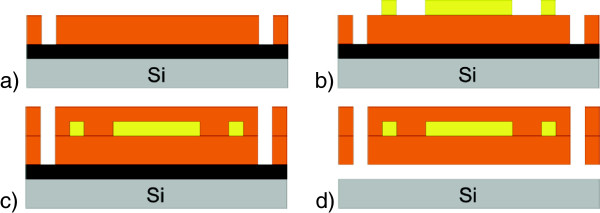
Figure 1.
Fabrication process of VLARS prototypes. a) 5 μm of polyimide spincoated and structured on Si-Wafer with sacrificial Al-layer (black), b) 2.5 μm of electroplated gold for wiring, c) another 5 μm of polyimide for isolation and protection of the wiring, d) after opening the second PI layer the electrodes are formed by another electroplating step. Further steps include: iridium oxide is sputtered and structured with a lift-off process, and the surface is coated with Parylene C, the electrodes are opened by a dry-etching process with oxygen plasma. Afterwards the devices are separated by etching the sacrificial Al-layer.

