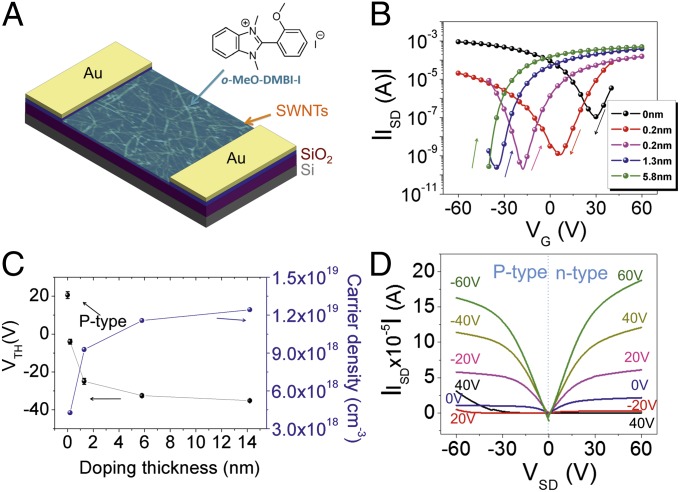
Fig. 1.
N-doping by vacuum evaporation. (A) Schematic of vacuum-evaporated o-MeO-DMBI-I doped SWNT TFTs (L = 20 μm, W = 400 μm). (B) Transfer characteristics of SWNT TFTs doped by o-MeO-DMBI-I at different nominal thicknesses determined by a quartz crystal monitor during deposition (VSD = 80 V for n-type and VSD = −80 V for p-type). (C) Average threshold voltage and calculated carrier density as a function of o-MeO-DMBI-I thickness. Five devices were characterized for each doping thickness, with error bars showing the standard deviation (SD) from the average value. (D) Output characteristics of undoped and n-doped SWNT TFTs at an o-MeO-DMBI-I thickness of 5.8 nm.

