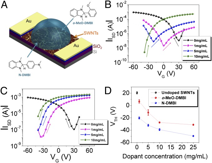
Fig. 2.
N-doping by solution deposited dopants. (A) Schematic of o-MeO-DMBI or N-DMBI doped SWNT TFTs prepared by solution doping (L = 20 μm, W = 400 μm). Transfer characteristics of SWNT TFTs doped by (B) o-MeO-DMBI and (C) N-DMBI, at different concentrations at VSD = 80V for n-type and VSD = −80V for p-type. (D) Average threshold voltage change as a function of various o-MeO-DMBI and N-DMBI concentrations. Five devices were measured for each doping concentration, with error bars showing the SD from the average value.

