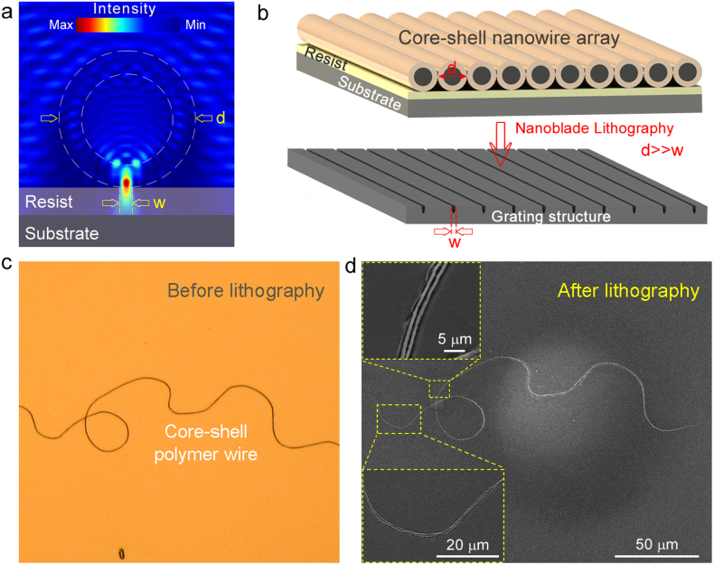
Figure 8. Photonic Nanoblade Lithography (PNL).
(a) Nano-blade lithography uses the focusing feature of NRM scattering in order to expose the photoresist in near subwavelength sizes. (b) Consequently, array of 1D grating structures or holes can be fabricated. (c) Single polymer wire used for the proof-of-concept demonstration of PNL technique. Polymer wire is laid on pre-coated photoresist. (d) After exposing sample into UV radiation and developing final structure, scheme of 1D nanohole imprinted original path is created. Thickness of polymer wire is 3.2 μm. The generated 1D hole possesses 400 nm widths.

