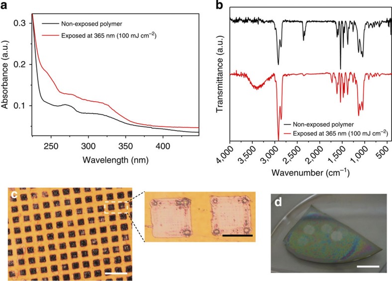
Figure 2. Polymer thin film photolysis studies.
(a) Characteristic ultraviolet/visible and (b) FT-IR spectra of the non-exposed and exposed polymer films at 365 nm radiation demonstrating typical absorbance and transmittance peaks of the photoproducts formed, (c) optical microscopy image showing the pattern formation after laser ablation of the polymer film with a single laser pulse (532 nm, 20 mJ cm−2) by application of a TEM grid as photomask; simultaneous Fresnel patterns in the squares of the photomask shown as a close-up image. Scale bar, 200 μm (expansion scale bar, 50 μm). (d) Digital photograph of the ablated areas that can be seen with the naked eye on a piece of a polymer coated silicon wafer. Scale bar, 10 mm.

