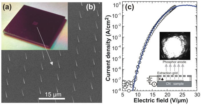
Figure 4.
(a) Optical micrograph of a fabricated 10 μm pitch CN array on a 10 × 10 mm Si substrate and the corresponding (b) scanning electron micrograph (Scale bar: 15 µm). (c) Measured current density as a function of applied electric field and the corresponding modelled emission with the inclusion of axial resistance, emitter degradation and know f(β) (solid line). The inset shows a schematic of the measurement diode setup and depicts the integrated optical intensity map, generated from phosphor coated ITO/glass, showing the spatial distribution in the emission.

