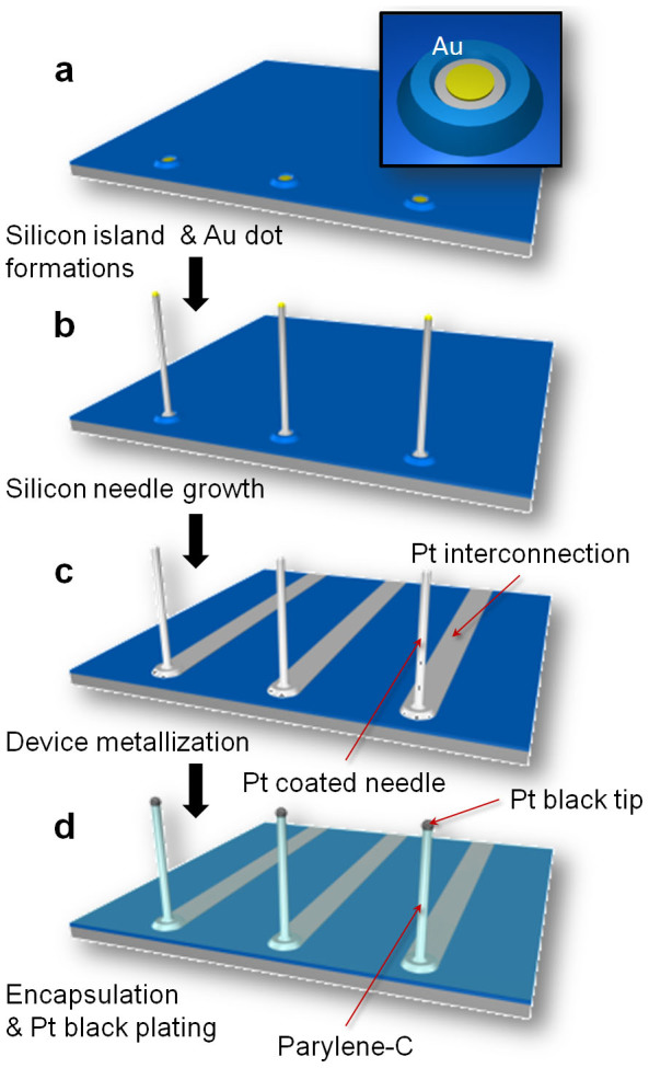
Figure 2. Schematics for device fabrication.

(a) Formation of silicon islands and preparation of catalytic-Au dots. (b) Au-catalyzed VLS growth of silicon needles. (c) Silicon needle metallization and formation of electrical interconnections by sputtering of Pt/Ti and a lift-off process. (d) Device encapsulation with an insulating layer of parylene-C. Tip section of the needle is exposed from the parylene-shell by a plasma process. After tip exposure, the Pt tip is electroplated with Pt black to realize low electrolyte/electrode interfacial electrical impedance characteristics.
